SNAS686 May 2016 TDC7201
PRODUCTION DATA.
- 1 Features
- 2 Applications
- 3 Description
- 4 Revision History
- 5 Pin Configuration and Functions
- 6 Specifications
-
7 Detailed Description
- 7.1 Overview
- 7.2 Functional Block Diagram
- 7.3 Feature Description
- 7.4 Device Functional Modes
- 7.5 Programming
- 7.6
Register Maps
- 7.6.1 Register Initialization
- 7.6.2 TDCx_CONFIG1: TDCx Configuration Register 1 R/W (address = 00h, CSBx asserted) [reset = 0h]
- 7.6.3 TDCx_CONFIG2: TDCx Configuration Register 2 R/W (address = 01h, CSBx asserted) [reset = 40h]
- 7.6.4 TDCx_INT_STATUS: Interrupt Status Register (address = 02h, CSBx asserted) [reset = 00h]
- 7.6.5 TDCx_INT_MASK: TDCx Interrupt Mask Register R/W (address = 03h, CSBx asserted) [reset = 07h]
- 7.6.6 TDCx_COARSE_CNTR_OVF_H: Coarse Counter Overflow High Value Register (address = 04h, CSBx asserted) [reset = FFh]
- 7.6.7 TDCx_COARSE_CNTR_OVF_L: TDCx Coarse Counter Overflow Low Value Register (address = 05h, CSBx asserted) [reset = FFh ]
- 7.6.8 TDCx_CLOCK_CNTR_OVF_H: Clock Counter Overflow High Register (address = 06h, CSBx asserted) [reset = FFh]
- 7.6.9 TDCx_CLOCK_CNTR_OVF_L: Clock Counter Overflow Low Register (address = 07h, CSBx asserted) [reset = FFh]
- 7.6.10 TDCx_CLOCK_CNTR_STOP_MASK_H: CLOCK Counter STOP Mask High Value Register (address = 08h, CSBx asserted) [reset = 00h]
- 7.6.11 TDCx_CLOCK_CNTR_STOP_MASK_L: CLOCK Counter STOP Mask Low Value Register (address = 09h, CSBx asserted) [reset = 00h]
- 7.6.12 TDCx_TIME1: Time 1 Register (address: 10h, CSBx asserted) [reset = 00_0000h]
- 7.6.13 TDCx_CLOCK_COUNT1: Clock Count Register (address: 11h, CSBx asserted) [reset = 00_0000h]
- 7.6.14 TDCx_TIME2: Time 2 Register (address: 12h, CSBx asserted) [reset = 00_0000h]
- 7.6.15 TDCx_CLOCK_COUNT2: Clock Count Register (address: 13h, CSBx asserted) [reset = 00_0000h]
- 7.6.16 TDCx_TIME3: Time 3 Register (address: 14h, CSBx asserted) [reset = 00_0000h]
- 7.6.17 TDCx_CLOCK_COUNT3: Clock Count Registers (address: 15h, CSBx asserted) [reset = 00_0000h]
- 7.6.18 TDCx_TIME4: Time 4 Register (address: 16h, CSBx asserted) [reset = 00_0000h]
- 7.6.19 TDCx_CLOCK_COUNT4: Clock Count Register (address: 17h, CSBx asserted) [reset = 00_0000h]
- 7.6.20 TDCx_TIME5: Time 5 Register (address: 18h, CSBx asserted) [reset = 00_0000h]
- 7.6.21 TDCx_CLOCK_COUNT5: Clock Count Register (address: 19h, CSBx asserted) [reset = 00_0000h]
- 7.6.22 TDCx_TIME6: Time 6 Register (address: 1Ah, CSBx asserted) [reset = 00_0000h]
- 7.6.23 TDCx_CALIBRATION1: Calibration 1 Register (address: 1Bh, CSBx asserted) [reset = 00_0000h]
- 7.6.24 TDCx_CALIBRATION2: Calibration 2 Register (address: 1Ch, CSBx asserted) [reset = 00_0000h]
- 8 Application and Implementation
- 9 Power Supply Recommendations
- 10Layout
- 11Device and Documentation Support
- 12Mechanical, Packaging, and Orderable Information
Package Options
Mechanical Data (Package|Pins)
- ZAX|25
Thermal pad, mechanical data (Package|Pins)
Orderable Information
10 Layout
10.1 Layout Guidelines
- In a 4-layer board design, the recommended layer stack order from top to bottom is: signal, ground, power and signal.
- Bypass capacitors should be placed in close proximity to the VDD pins.
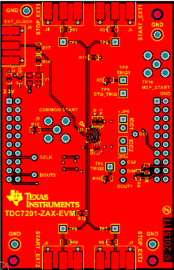
- The length of the START and STOP traces from the TDC7201 to the AFE or MCU should be matched to prevent uneven signal delays. Also, avoid unnecessary via-holes on these traces and keep the routing as short and direct as possible to minimize parasitic capacitance on the PCB.
- Route the SPI signal traces close together. Place a series resistor at the source of DOUT (close to the TDC7201) and series resistors at the sources of DIN, SCLK, and CSB (close to the master MCU).
10.2 Layout Example
 Figure 56. TDC7201EVM Layout