SLES032E June 2002 – September 2014 THS8200
PRODUCTION DATA.
- 1 Device Overview
- 2 Revision History
- 3 Terminal Configuration and Functions
-
4 Specifications
- 4.1 Absolute Maximum Ratings
- 4.2 Handling Ratings
- 4.3 Recommended Operating Conditions
- 4.4 Power Consumption Summary
- 4.5 Power Supply
- 4.6 Digital Inputs, DC Characteristics
- 4.7 Analog (DAC) Outputs
- 4.8 Nonlinearity
- 4.9 Analog Output Bandwidth (sinx/x corrected) at fS = 205 MSPS
- 4.10 Output Compliance vs Full-Scale Adjustment Resistor Value
- 4.11 Vertical Sync of the HDTV 1080I Format Preset in First and Second Field, and Horizontal Line Waveform Detail
-
5 Functional Overview
- 5.1
Data Manager (DMAN)
- 5.1.1 Interpolating Finite Impulse Responses Filter (IFIR)
- 5.1.2 Color-Space Conversion (CSC)
- 5.1.3 Clip/Shift/Multiplier (CSM)
- 5.1.4 Digital Multiplexer (DIGMUX)
- 5.1.5 Display Timing Generator (DTG)
- 5.1.6 Clock Generator (CGEN)
- 5.1.7 Clock Driver (CDRV)
- 5.1.8 I2C Host Interface (I2CSLAVE)
- 5.1.9 Test Block (TST)
- 5.1.10 D/A Converters (DACs)
- 5.1
Data Manager (DMAN)
-
6 Detailed Functional Description
- 6.1 Data Manager (DMAN)
- 6.2 Input Interface Formats
- 6.3 Clock Generator (CGEN)/Clock Driver (CDRV)
- 6.4 Color Space Conversion (CSC)
- 6.5 Clip/Shift/Multiplier (CSM)
- 6.6 Interpolating Finite Impulse Response Filter (IFIR)
- 6.7
Display Timing Generator (DTG)
- 6.7.1 Overview of Functionality
- 6.7.2 Functional Description
- 6.7.3
DTG Line Type Overview
- 6.7.3.1 HDTV Mode
- 6.7.3.2 Active Video
- 6.7.3.3 FULL NTSP (Full Normal Tri-Level Sync Pulse)
- 6.7.3.4 NTSP NTSP (Normal Tri-Level Sync Pulse/Normal Tri-Level Sync Pulse)
- 6.7.3.5 BTSP BTSP (Broad Pulse and Tri-Level Sync Pulse/Broad Pulse and Tri-Level Sync Pulse)
- 6.7.3.6 NTSP BTSP (Normal Tri-Level Sync Pulse/ Broad Pulse and Tri-Level Sync Pulse)
- 6.7.3.7 BTSP NTSP (Broad Pulse and Tri-Level Sync Pulse/Normal Tri-Level Sync Pulse)
- 6.7.3.8 Full BTSP (Full Broad Pulse and Tri-Level Sync Pulse)
- 6.7.3.9 SDTV Mode
- 6.7.3.10 NEQ_NEQ (Negative Equalization Pulse/Negative Equalization Pulse)
- 6.7.3.11 FULL_BSP (Full Broad Sync Pulse)
- 6.7.3.12 BSP_BSP (Broad Sync Pulse/Broad Sync Pulse)
- 6.7.3.13 FULL_NSP (Full Normal Sync Pulse)
- 6.7.3.14 NEQ_BSP (Negative Equalization Pulse/Broad Sync Pulse)
- 6.7.3.15 BSP_NEQ (Broad Sync Pulse/Negative Equalization Pulse)
- 6.7.3.16 FULL_NEQ (Full Negative Equalization Pulse)
- 6.7.3.17 NSP_ACTIVE (Normal Sync Pulse/Active Video)
- 6.7.3.18 ACTIVE_NEQ (Active Video/Negative Equalization Pulse)
- 6.7.3.19 ACTIVE VIDEO
- 6.8
D/A Conversion
- 6.8.1 RGB Output Without Sync Signal Insertion/General-Purpose Application DAC
- 6.8.2 SMPTE-Compatible RGB Output With Sync Signal Inserted on G (Green) Channel
- 6.8.3 SMPTE-Compatible Analog-Level Output With Sync Inserted on All RGB Channels
- 6.8.4 SMPTE-Compatible YPbPr Output With Sync Signal Inserted on Y Channel Only
- 6.8.5 SMPTE-Compatible YPbPr Output With Sync Signal Inserted on All Channels
- 6.8.6 Summary of Supported Video Formats
- 6.9 Test Functions
- 6.10 Power Down
- 6.11 CGMS Insertion
- 6.12 I2C Interface
-
7 I2C Registers
- 7.1 I2C Register Map
- 7.2
Register Descriptions
- 7.2.1 System Control (Sub-Addresses 0x02−0x03)
- 7.2.2 Color Space Conversion Control (Sub-Addresses 0x04−0x19)
- 7.2.3 Test Control (Sub-Addresses 0x1A−0x1B)
- 7.2.4 Data Path Control (Sub-Address 0x1C)
- 7.2.5 Display Timing Generator Control, Part 1 (Sub-Addresses 0x1D−0x3C)
- 7.2.6 DAC Control (Sub-Addresses 0x3D−0x40)
- 7.2.7 Clip/Shift/Multiplier Control (Sub-Addresses 0x41−0x4F)
- 7.2.8 Display Timing Generator Control, Part 2 (Sub-Addresses 0x50−0x82)
- 7.2.9 CGMS Control (Sub-Addresses 0x83−0x85)
- 7.3 THS8200 Preset Mode Line Type Definitions
- 8 Application Information
- 9 Device and Documentation Support
- 10Mechanical, Packaging, and Orderable Information
Package Options
Mechanical Data (Package|Pins)
- PFP|80
Thermal pad, mechanical data (Package|Pins)
- PFP|80
Orderable Information
1 Device Overview
1.1 Features
- Overall
- Three 11-Bit 205-MSPS Digital-to-Analog Converters (DACs) With Integrated Bi-Level or Tri-Level Sync Insertion
- Support for All ATSC Video Formats (Including 1080P) and PC Graphics Formats (up to UXGA at 75 Hz)
- Input
- Flexible 10-, 15-, 16-, 20-, 24-, or 30-Bit Digital Video Input Interface With Support for YCbCr or RGB Data, Either 4:4:4 or 4:2:2 Sampled
- Video Synchronization by Hsync or Vsync Dedicated Inputs or by Extraction of Embedded SAV and EAV Codes According to ITU-R.BT601 (SDTV) or SMPTE 274M and SMPTE 296M (HDTV)
- Glueless Interface to TI DVI 1.0 (With HDCP) Receivers. Can Receive Video-Over-DVI Formats According to the EIA-861 Specification and Convert to YPbPr or RGB Component Formats With Separate Syncs or Embedded Composite Sync.
- Video Processing
- Programmable Clip/Shift/Multiply Function for Operation With Full-Range or ITU-R.BT601 Video Range Input Data
- Programmable Digital Fine-Gain Controller on Each Analog Output Channel, for Accurate Channel Matching and Programmable White-Balance Control
- Built-In 4:2:2 to 4:4:4 Video Interpolation Filter
- Built-In 2x Oversampling SDTV and HDTV Interpolation Filter for Improved Video Frequency Characteristic
- Fully Programmable Digital Color Space Conversion Circuit
- Fully Programmable Display Timing Generator to Supply All SDTV and HDTV Composite Sync Timing Formats, Progressive and Interlaced
- Fully Programmable Hsync and Vsync Outputs
- Vertical Blanking Interval (VBI) Override or Data Pass-Through for VBI Data Transparency
- Programmable CGMS Data Generation and Insertion
- Output
- Digital
- ITU-R BT.656 Digital Video Output Port
- Analog
- Analog Component Output from Software-Switchable 700-mV or 1.3-V Compliant Output DACs at 37.5-Ω Load
- Programmable Video/Sync Ratio (7:3 or 10:4)
- Programmable Video Pedestal
- Digital
- General
- Built-In Video Color Bar Test Pattern Generator
- Fast Mode I2C Control Interface
- Configurable Master or Slave Timing Mode
- Configuration Modes Allow the Device to Act as a Master Timing Source for Requesting Data From, for Example, the Video Frame Buffer (Master Mode Only Available for PC Graphics Output Modes).
- Alternatively, the Device Can Slave to an External Timing Master.
- DAC and Chip Power-Down Modes
- Low-Power 1.8-V and 3.3-V Operation
- 80-Pin PowerPAD™ Plastic Quad Flatpack Package With Efficient Heat Dissipation and Small Physical Size
1.2 Applications
- DVD Players
- Digital-TV, Interactive-TV, or Internet Set-Top Boxes
- Personal Video Recorders
- HDTV Display or Projection Systems
- Digital Video Systems
1.3 Description
The THS8200 device is a complete video back-end D/A solution for DVD players, personal video recorders and set-top boxes, or any system requiring the conversion of digital component video signals into the analog domain.
The THS8200 device can accept a variety of digital input formats, in 4:4:4 and 4:2:2 formats, over an interface of three, two, or one 10‑bit ports. The device synchronizes to incoming video data either through dedicated Hsync and Vsync inputs or through extraction of the sync information from embedded sync (SAV and EAV) codes inside the video stream. Alternatively, when the THS8200 is configured for generating PC graphics output, the device also provides a master timing mode in which it requests video data from an external (memory) source.
The THS8200 device contains a display timing generator that is completely programmable for all standard and nonstandard video formats up to the maximum supported pixel clock of 205 MSPS. Therefore, the device supports all component video and PC graphics (VESA) formats. A fully programmable 3x3 matrixing operation is included for color space conversion. All video formats, up to the HDTV 1080I and 720P formats, can also be internally 2x oversampled. Oversampling relaxes the need for sharp external analog reconstruction filters behind the DAC and improves the video frequency characteristic.
The output compliance range can be set through external adjustment resistors, and there is a choice of two settings to accommodate both component video or PC graphics (700-mV) and composite video (1.3‑V) outputs without hardware changes. An internal programmable clip/shift/multiply function on the video data assures standards-compliant video output ranges for either full 10-bit or reduced ITU-R.BT601 style video input. To avoid nonlinearities after scaling of the video range, the DACs have 11-bit resolution internally. Furthermore, a bi-level or tri-level sync with programmable amplitude (to support both 700-mV:300-mV and 714-mV:286-mV video:sync ratios) can be inserted either on the green/luma channel only or on all three output channels. This sync insertion is generated from additional current sources in the DACs such that the full DAC resolution remains available for the video range and preserves 100% of the 11-bit dynamic range of the DAC for video data.
The THS8200 optionally supports the pass-through of ancillary data embedded in the input video stream or can insert ancillary data into the 525P analog component output according to the CGMS data specification.
Device Information(1)
| PART NUMBER | PACKAGE | BODY SIZE(2) |
|---|---|---|
| THS8200PFP | HTQFP (80) | 12 mm x 12 mm |
1.4 Functional Block Diagram
Figure 1-1 shows the functional block diagram.
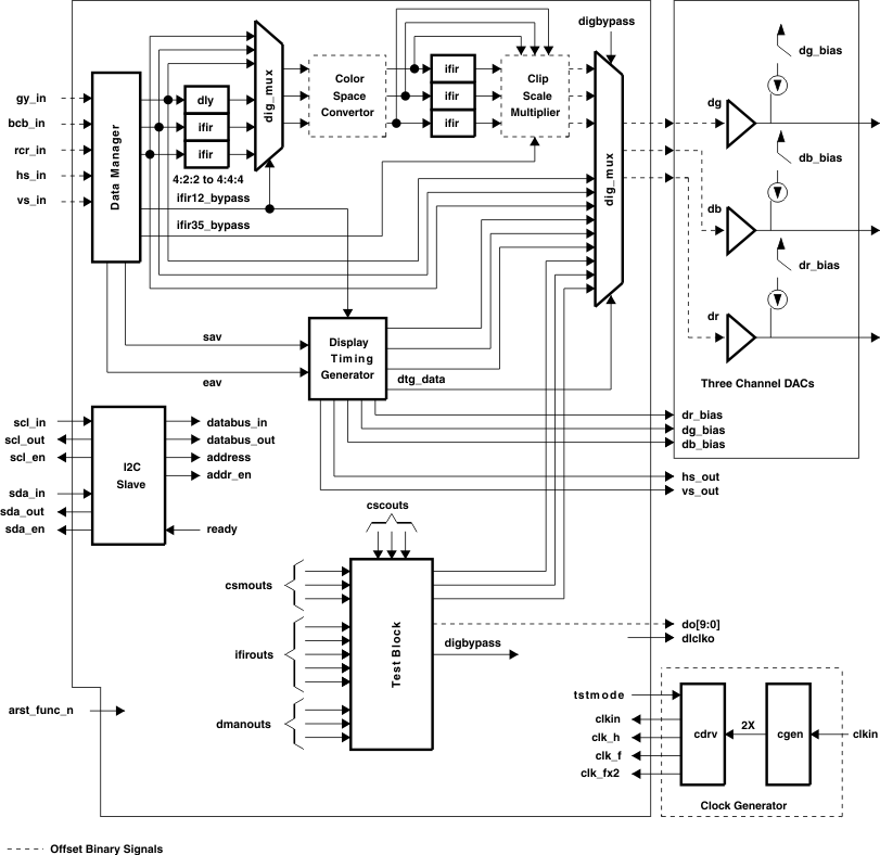 Figure 1-1 Functional Block Diagram