SLVSA51E March 2010 – September 2016 TLC5940-EP
PRODUCTION DATA.
- 1 Features
- 2 Applications
- 3 Description
- 4 Revision History
- 5 Pin Configuration and Functions
- 6 Specifications
- 7 Parameter Measurement Information
- 8 Detailed Description
- 9 Application and Implementation
- 10Power Supply Recommendations
- 11Layout
- 12Device and Documentation Support
- 13Mechanical, Packaging, and Orderable Information
Package Options
Mechanical Data (Package|Pins)
Thermal pad, mechanical data (Package|Pins)
Orderable Information
1 Features
- 16 Channels
- 12-Bit (4096 Steps) Grayscale PWM Control
- Dot Correction
- 6 Bit (64 Steps)
- Storable in Integrated EEPROM
- Drive Capability (Constant-Current Sink) of
0 mA to 72 mA (–40°C to 125°C)- 0 mA to 60 mA (VCC < 3.6 V, –40°C to 85°C)
- 0 mA to 120 mA (VCC > 3.6 V, –40°C to 85°C)
- LED Power Supply Voltage up to 17 V
- VCC = 3 V to 5.5 V
- Serial Data Interface
- Controlled In-Rush Current
- 30-MHz Data Transfer Rate
- CMOS Level I/O
- Error Information
- LOD: LED Open Detection
- TEF: Thermal Error Flag
2 Applications
- Monocolor, Multicolor, Full-Color LED Displays
- LED Signboards
- Display Backlighting
- General, High-Current LED Drive
- Supports Defense, Aerospace, and Medical Applications:
- Controlled Baseline
- One Assembly/Test Site
- One Fabrication Site
- Available in Q-Temp (–40°C/125°C)
- Extended Product Life Cycle
- Extended Product-Change Notification
- Product Traceability
3 Description
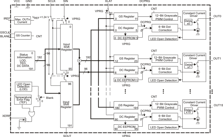
The TLC5940-EP is a 16-channel, constant-current sink LED driver. Each channel has an individually adjustable 4096-step grayscale PWM brightness control and a 64-step, constant-current sink (dot correction). The dot correction adjusts the brightness variations between LED channels and other LED drivers. The dot correction data is stored in an integrated EEPROM. Both grayscale control and dot correction are accessible via a serial interface. A single external resistor sets the maximum current value of all 16 channels.
The TLC5940-EP features two error information circuits. The LED open detection (LOD) indicates a broken or disconnected LED at an output terminal. The thermal error flag (TEF) indicates an overtemperature condition.
Device Information(1)
| PART NUMBER | PACKAGE | BODY SIZE (NOM) |
|---|---|---|
| TLC5940-EP | HTSSOP (28) | 9.70 mm × 4.40 mm |
| VQFN (32) | 5.00 mm × 5.00 mm |
- For all available packages, see the orderable addendum at the end of the data sheet.
Simplified Schematic

4 Revision History
Changes from D Revision (May 2010) to E Revision
- Added ESD Ratings table, Feature Description section, Device Functional Modes, Application and Implementation section, Power Supply Recommendations section, Layout section, Device and Documentation Support section, and Mechanical, Packaging, and Orderable Information section Go
- Deleted Ordering Information table; see POA at the end of the data sheetGo
- Changed thermal values for RHB (VQFN) package: 33.9 to 36.7 for RθJA, 30 to 18.9 for RθJC(top), 9.3 to 15.9 for RθJB, 0.619 to 0.6 for ψJT, 9.3 to 15.8 for ψJB, and 3.9 to 2.3 for RθJC(bot)Go
- Changed thermal values for PWP (HTSSOP) package: 35.4 to 34.3 for RθJA, 24.94 to 36.8 for RθJC(top), 15.02 to 8.5 for RθJB, 1.297 to 0.3 for ψJT, 10.96 to 8.7 for ψJB, and 5.37 to 1.6 for RθJC(bot)Go
- Deleted Dissipation Ratings tableGo
Changes from B Revision (September 2007) to C Revision
- Changed from ms to nsGo