SBOS858 April 2017 TLV171-Q1
PRODUCTION DATA.
- 1 Features
- 2 Applications
- 3 Description
- 4 Description (continued)
- 5 Pin Configuration and Functions
- 6 Specifications
- 7 Detailed Description
- 8 Application and Implementation
- 9 Power Supply Recommendations
- 10Layout
- 11Device and Documentation Support
- 12Mechanical, Packaging, and Orderable Information
Package Options
Mechanical Data (Package|Pins)
- DBV|5
Thermal pad, mechanical data (Package|Pins)
Orderable Information
7 Detailed Description
7.1 Overview
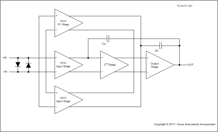
The TLVx171-Q1 family of operational amplifiers provides high overall performance, making them ideal for many general-purpose applications. The excellent offset drift of only 1 µV/°C (typical) provides excellent stability over the entire temperature range. In addition, the device offers very good overall performance with high CMRR, PSRR, AOL, and superior THD.
7.2 Functional Block Diagram

7.3 Feature Description
7.3.1 Operating Characteristics
The TLVx171-Q1 family of devices is specified for operation from 4.5 V to 36 V (±2.25 V to ±18 V). Many of the specifications apply from –40°C to +125°C. Parameters that can exhibit significant variance with regard to operating voltage or temperature are shown in Typical Characteristics.
7.3.2 Phase-Reversal Protection
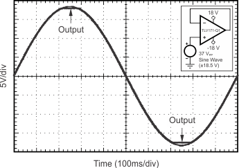
The TLVx171-Q1 family of devices has an internal phase-reversal protection. Many op amps exhibit a phase reversal when the input is driven beyond the linear common-mode range. This condition is most often encountered in noninverting circuits when the input is driven beyond the specified common-mode voltage range, causing the output to reverse into the opposite rail. The input of the TLVx171-Q1 family of devices prevents phase reversal with excessive common-mode voltage. Instead, the output limits into the appropriate rail. Figure 26 shows this performance.
 Figure 26. No Phase Reversal
7.3.3 Capacitive Load and Stability
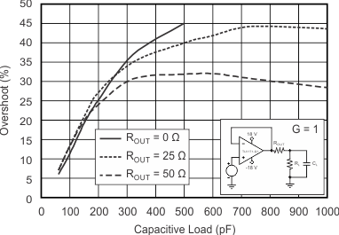
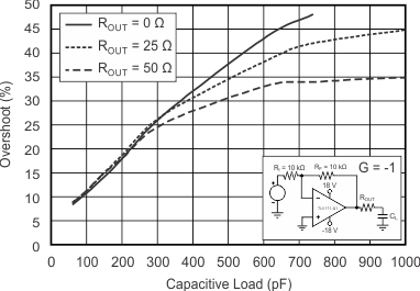
The dynamic characteristics of the TLVx171-Q1 family of devices are optimized for commonly encountered operating conditions. The combination of low closed-loop gain and high capacitive loads decreases the phase margin of the amplifier and can lead to gain peaking or oscillations. As a result, heavier capacitive loads must be isolated from the output. The simplest way to achieve this isolation is to add a small resistor (for example, ROUT equal to 50 Ω) in series with the output. Figure 27 and Figure 28 shows small-signal overshoot versus capacitive load for several values of ROUT. For details of analysis techniques and application circuits, see Applications Bulletin AB-028, available for download from TI.com.

| RL = 10 kΩ |

7.4 Device Functional Modes
7.4.1 Common-Mode Voltage Range
The input common-mode voltage range of the TLVx171-Q1 family of devices extends 100 mV below the negative rail and within 2 V of the top rail for normal operation.
This device can operate with full rail-to-rail input 100 mV beyond the top rail, but with reduced performance within 2 V of the top rail. The typical performance in this range is listed in Table 3.
Table 3. Typical Performance Range
| PARAMETER | MIN | TYP | MAX | UNIT | |
|---|---|---|---|---|---|
| Input common-mode voltage | (V+) – 2 | (V+) + 0.1 | V | ||
| Offset voltage | 7 | mV | |||
| Offset voltage vs temperature | 12 | µV/°C | |||
| Common-mode rejection | 65 | dB | |||
| Open-loop gain | 60 | dB | |||
| GBW | 0.7 | MHz | |||
| Slew rate | 0.7 | V/µs | |||
| Noise at f = 1kHz | 30 | nV/√Hz | |||