SLAS579A April 2009 – June 2015 TLV2553-Q1
PRODUCTION DATA.
- 1 Features
- 2 Applications
- 3 Description
- 4 Revision History
- 5 Pin Configuration and Functions
-
6 Specifications
- 6.1 Absolute Maximum Ratings
- 6.2 ESD Ratings
- 6.3 Recommended Operating Conditions
- 6.4 Thermal Information
- 6.5 Electrical Characteristics
- 6.6 External Reference Specifications
- 6.7 Operating Characteristics
- 6.8 Timing Requirements, VREF+ = 5 V
- 6.9 Timing Requirements, VREF+ = 2.5 V
- 6.10 Typical Characteristics
- 7 Parameter Measurement Information
-
8 Detailed Description
- 8.1 Overview
- 8.2 Functional Block Diagram
- 8.3 Feature Description
- 8.4 Device Functional Modes
- 9 Application and Implementation
- 10Power Supply Recommendations
- 11Layout
- 12Device and Documentation Support
- 13Mechanical, Packaging, and Orderable Information
Package Options
Mechanical Data (Package|Pins)
Thermal pad, mechanical data (Package|Pins)
- PW|20
Orderable Information
1 Features
- Qualified for Automotive Applications
- 12-Bit-Resolution Analog-to-Digital Converter (ADC)
- Up to 200-KSPS (150-KSPS for 3 V) Throughput Over Operating Temperature Range With 12-Bit Output Mode
- 11 Analog Input Channels
- Three Built-In Self-Test Modes
- Inherent Sample and Hold Function
- Linearity Error of +1 LSB (Max)
- On-Chip Conversion Clock
- Unipolar or Bipolar Output Operation
- Programmable Most Significant Bit (MSB) or Least Significant Bit (LSB) First
- Programmable Power Down
- Programmable Output Data Length
- SPI Compatible Serial Interface With I/O Clock Frequencies up to 15 MHz (CPOL = 0, CPHA = 0)
2 Applications
- Process Control
- Portable Data Logging
- Battery-Powered Instruments
- Automotive
3 Description
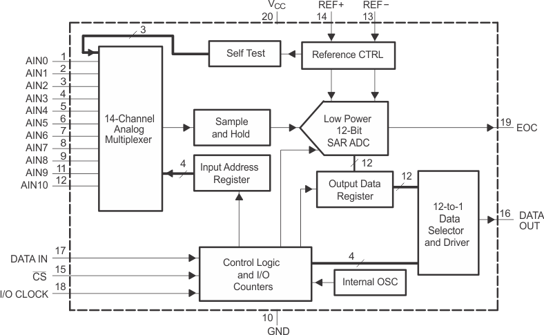
The TLV2553-Q1 is a 12-bit switched-capacitor successive-approximation analog-to-digital converter (ADC). The ADC has three control inputs [chip select (CS), the input-output clock, and the address/control input (DATAIN)] designed for communication with the serial port of a host processor or peripheral through a serial 3-state output.
In addition to the high-speed converter and versatile control capability, the device has an on-chip 14-channel multiplexer that can select any one of 11 inputs or any one of three internal self-test voltages using configuration register 1. The sample-and-hold function is automatic. At the end of conversion, when programmed as EOC, the pin 19 output goes high to indicate that conversion is complete. The converter incorporated in the device features differential high-impedance reference inputs that facilitate ratiometric conversion, scaling, and isolation of analog circuitry from logic and supply noise. A switched-capacitor design allows low-error conversion over the full operating temperature range.
The TLV2553-Q1 is characterized for operation from TA = –40°C to 85°C.
Device Information(1)
| PART NUMBER | PACKAGE | BODY SIZE (NOM) |
|---|---|---|
| TLV2553-Q1 | SOIC (20) | 7.50 mm × 12.80 mm |
| TSSOP (20) | 4.40 mm × 6.50 mm |
- For all available packages, see the orderable addendum at the end of the data sheet.
Block Diagram
