SBOS694A December   2013  – November 2015 TLV3691

PRODUCTION DATA.  

  1. Features
  2. Applications
  3. Description
  4. Revision History
  5. Pin Configuration and Functions
  6. Specifications
    1. 6.1 Absolute Maximum Ratings
    2. 6.2 ESD Ratings
    3. 6.3 Recommended Operating Conditions
    4. 6.4 Thermal Information
    5. 6.5 Electrical Characteristics
    6. 6.6 Switching Characteristics
    7. 6.7 Typical Characteristics
  7. Detailed Description
    1. 7.1 Overview
    2. 7.2 Functional Block Diagram
    3. 7.3 Feature Description
    4. 7.4 Device Functional Modes
      1. 7.4.1 Nano-Power
      2. 7.4.2 Rail-to-Rail Inputs
      3. 7.4.3 Push-Pull Output
  8. Application and Implementation
    1. 8.1 Application Information
      1. 8.1.1 Comparator Inputs
      2. 8.1.2 External Hysteresis
        1. 8.1.2.1 Inverting Comparator With Hysteresis
        2. 8.1.2.2 Noninverting Comparator With Hysteresis
      3. 8.1.3 Capacitive Loads
      4. 8.1.4 Setting the Reference Voltage
    2. 8.2 Typical Application
      1. 8.2.1 Window Comparator
        1. 8.2.1.1 Design Requirements
        2. 8.2.1.2 Detailed Design Procedure
        3. 8.2.1.3 Application Curve
      2. 8.2.2 Overvoltage and Undervoltage Detection
  9. Power Supply Recommendations
  10. 10Layout
    1. 10.1 Layout Guidelines
    2. 10.2 Layout Example
  11. 11Device and Documentation Support
    1. 11.1 Device Support
      1. 11.1.1 Development Support
        1. 11.1.1.1 TINA-TI (Free Software Download)
        2. 11.1.1.2 TI Precision Designs
    2. 11.2 Documentation Support
      1. 11.2.1 Related Documentation
    3. 11.3 Community Resources
    4. 11.4 Trademarks
    5. 11.5 Electrostatic Discharge Caution
    6. 11.6 Glossary
  12. 12Mechanical, Packaging, and Orderable Information

Package Options

Mechanical Data (Package|Pins)
Thermal pad, mechanical data (Package|Pins)
Orderable Information

5 Pin Configuration and Functions

DCK Package
5-Pin SC70
Top View
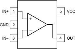
TLV3691 po_sc70_bos694.gif
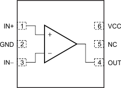
DPF Package
6-Pin X2SON
Top View
TLV3691 po_son_bos694.gif

Pin Functions

PIN I/O DESCRIPTION
NAME X2SON SC70
GND 2 2 Ground
IN+ 1 1 I Noninverting input
IN– 3 3 I Inverting input
NC 5 No internal connection
OUT 4 4 O Output (push-pull)
VCC 6 5 I Positive power supply