SNVSAV1A June 2017 – October 2017 TLV760
PRODUCTION DATA.
- 1 Features
- 2 Applications
- 3 Description
- 4 Revision History
- 5 Pin Configuration and Functions
- 6 Specifications
- 7 Detailed Description
- 8 Application and Implementation
- 9 Power Supply Recommendations
- 10Layout
- 11Device and Documentation Support
- 12Mechanical, Packaging, and Orderable Information
Package Options
Mechanical Data (Package|Pins)
- DBZ|3
Thermal pad, mechanical data (Package|Pins)
Orderable Information
8 Application and Implementation
NOTE
Information in the following applications sections is not part of the TI component specification, and TI does not warrant its accuracy or completeness. TI’s customers are responsible for determining suitability of components for their purposes. Customers should validate and test their design implementation to confirm system functionality.
8.1 Application Information
The TLV760 is a fixed output device which need only input and output capacitors to function. This section discusses the key aspects to implement this linear regulator in typical applications.
8.1.1 Fixed Output
TLV760 comes in fixed output voltage options, 3.3 V, 5 V, 12 V and 15 V. To ensure the proper regulated output, the input voltage should be greater than VOUT(nom) + VDO.
8.1.2 External Capacitors
8.1.2.1 Input and Output Capacitor Requirements
A minimum input and output capacitance value of 0.1 µF is required for stability and adequate transient performance. There is no specific equivalent series resistance (ESR) limitation, although excessively high ESR compromises transient performance. There is no specific limitation on a maximum capacitance value on the input or the output. However while selecting a capacitor, derating factors on the capacitance value should be considered. Use C0G, X7R, or X5R-type ceramic capacitors because these capacitors have minimal variation in capacitance value and ESR over temperature.
8.1.2.2 Load-Step Transient Response
The load-step transient response is the output voltage response by the linear regulator to a step change in load current. The depth of charge depletion immediately after the load step is directly proportional to the amount of output capacitance. However, larger output capacitances decrease any voltage dip or peak occurring during a load step, the control-loop bandwidth is also decreased, thereby slowing the response time. TI recommends to optimally scale output capacitors for a specific application and test for the output load transients.
8.1.3 Power Dissipation
Proper consideration should be given to device power dissipation, location of the circuit on the printed circuit board (PCB), and correct sizing of the thermal plane to ensure the device reliability. The PCB area around the regulator must be as free as possible of other heat-generating devices that cause added thermal stresses. To first-order approximation, power dissipation in the regulator depends on the input-to-output voltage difference and load conditions. Power dissipation can be calculated using The thermal protection follows Equation 1:

where
- PD = (VIN – VOUT )IOUT
- TJ is the junction temperature
- RθJA is the junction-to-ambient thermal resistance
Thus, at a given load current, input and output voltage, maximum power dissipation determines the maximum allowable ambient temperature (TA) for the device, and vice versa. Power dissipation and junction temperature are most often related by the junction-to-ambient thermal resistance (RθJA) of the combined PCB and device package and the temperature of the ambient air (TA).
RθJA is highly dependent on the heat-spreading capability built into the particular PCB design, and therefore varies according to the total copper area, copper weight, and location of the planes. The RθJA recorded in Thermal Information is determined by the JEDEC standard, PCB, and copper-spreading area and is only used as a relative measure of package thermal performance.
TLV760 integrates a rugged protection where the TJ is limited to 150°C. The maximum power dissipation depends on the ambient temperature and can be calculated using PD = (TJ – TA) / RθJA, for example, substituting the absolute maximum junction temperature, 150°C for TJ, 50°C for TA, and 275.2 °C/W for RθJA, the maximum power that can be dissipated is 363 mW. More power can be safely dissipated at lower ambient temperatures. Less power can be safely dissipated at higher ambient temperatures. The power dissipation can be increased by 3.6 mW for each °C below 50°C ambient. It must be derated by 3.6 mW for each °C above 50°C ambient. Proper heat sinking enables the safe dissipation of more power.
8.2 Typical Application
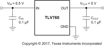 Figure 18. Typical Appication for the 5-V Option
8.2.1 Design Requirements
For typical TLV760 applications, use the parameters in Table 1.
Table 1. Design Parameters
| DESIGN PARAMETER | EXAMPLE VALUE |
|---|---|
| Input voltage | 6.5 V |
| Output voltage | 5 V |
| Output current | 100 mA |
8.2.2 Detailed Design Procedure
The output for TLV76050 is internally set to 5 V. Input and output capacitors can be selected in accordance with the External Capacitors. Ceramic capacitances of 0.1 µF for both input and output are selected.
See the Layout section for an example of how to PCB layout the TLV760 to achieve best performance.
8.2.3 Application Curves
Unless indicated otherwise, VIN = 6.5 V, VOUT = 5 V, COUT = 0.1 µF, and TA = 25°C.
 Figure 19. Line Transient Response
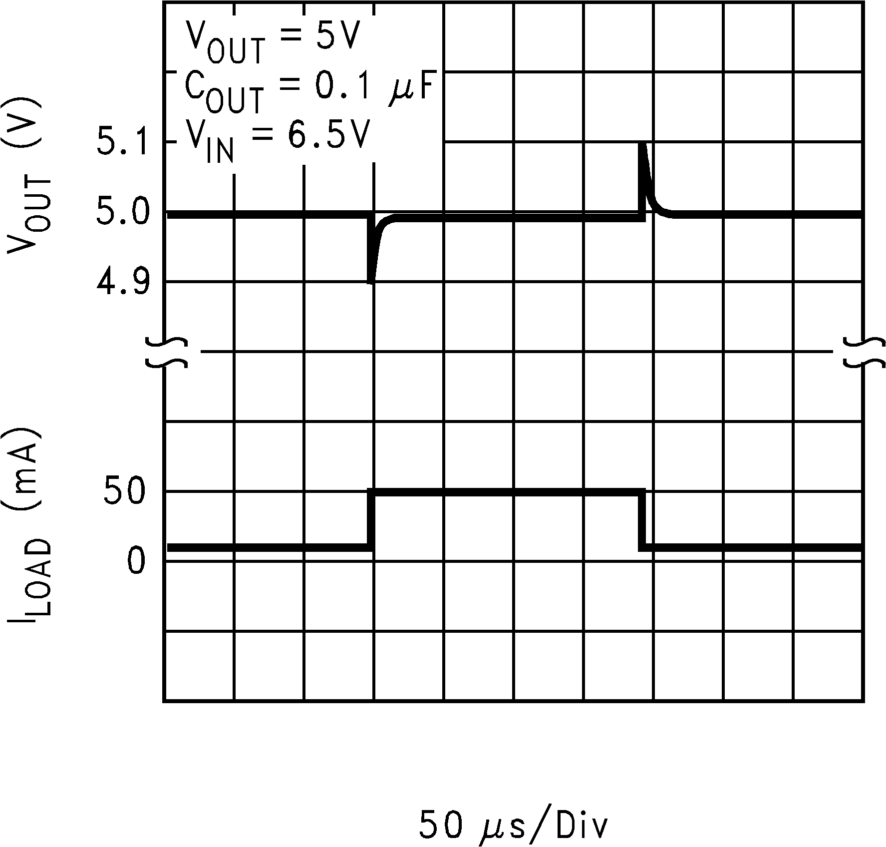 Figure 21. Load Transient Response
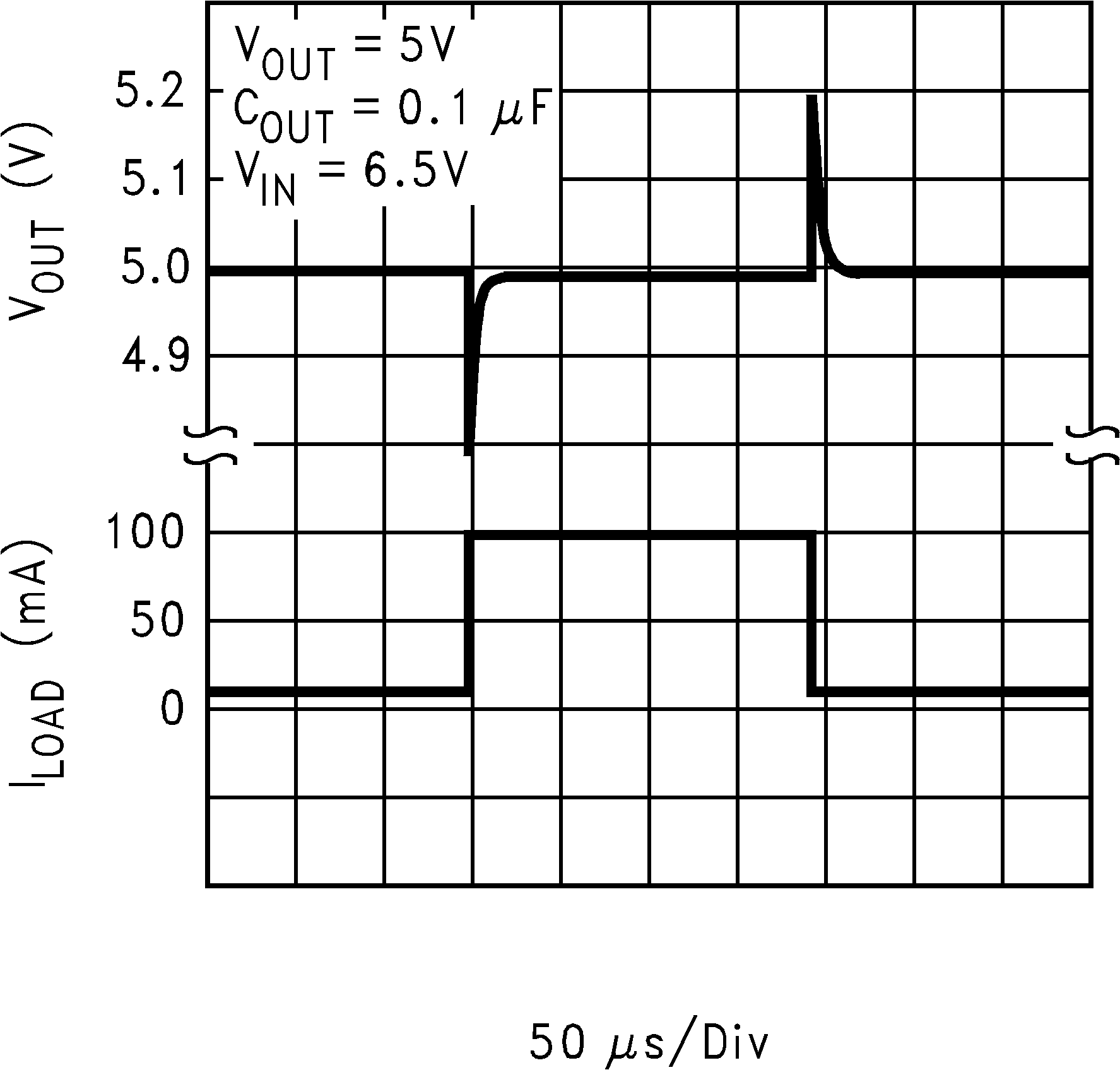 Figure 23. Load Transient Response
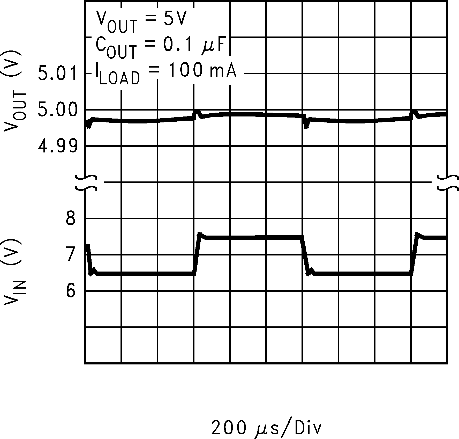 Figure 20. Line Transient Response
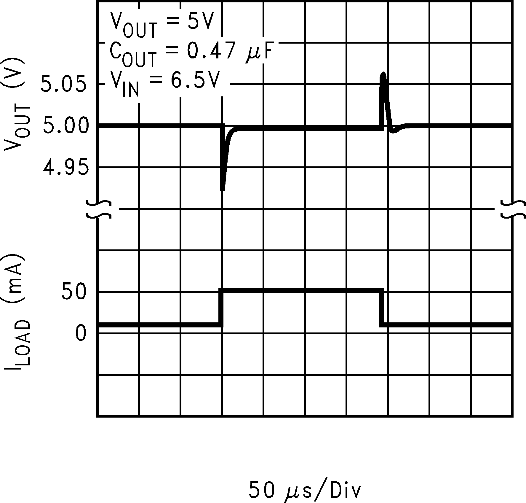 Figure 22. Load Transient Response
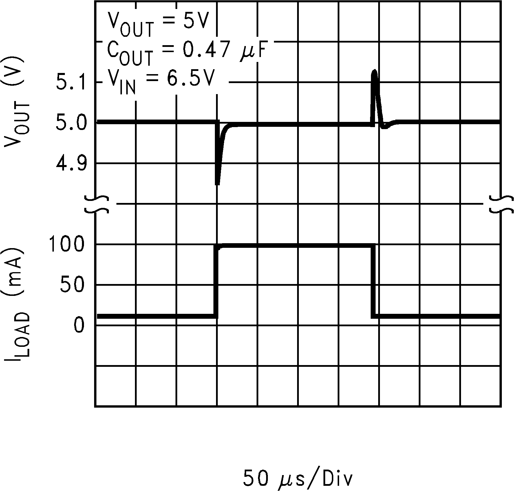 Figure 24. Load Transient Response