SBOS518E May 2011 – April 2015 TMP006
PRODUCTION DATA.
- 1 Features
- 2 Applications
- 3 Description
- 4 Revision History
- 5 Device Comparison Table
- 6 Pin Configuration and Functions
- 7 Specifications
-
8 Detailed Description
- 8.1 Overview
- 8.2 Functional Block Diagram
- 8.3 Feature Description
- 8.4 Device Functional Modes
- 8.5 Register Maps
- 9 Application and Implementation
- 10Power-Supply Recommendations
- 11Layout
- 12Device and Documentation Support
- 13Mechanical, Packaging, and Orderable Information
Package Options
Mechanical Data (Package|Pins)
- YZF|8
Thermal pad, mechanical data (Package|Pins)
Orderable Information
9 Application and Implementation
NOTE
Information in the following applications sections is not part of the TI component specification, and TI does not warrant its accuracy or completeness. TI’s customers are responsible for determining suitability of components for their purposes. Customers should validate and test their design implementation to confirm system functionality.
9.1 Application Information
The TMP006 and TMP006B are a complete IR thermopile sensor system on a chip that includes the sensing element, signal conditioner, and ADC. These devices are ideal for applications where the object cannot be placed in thermal contact with a conventional temperature sensor. Common reasons for noncontact temperature sensing are:
- Distance; the object is too far away, or in an inconvenient location for wired connections.
- The object is in motion.
- Direct contact of the object is inconvenient or uncomfortable (for example, skin).
- The object is a fluid (that is, liquid or gas).
- The object is hazardous (for example, acid or flammable).
- The object is in a hazardous state (for example, high voltage).
9.2 Typical Application
9.2.1 Wide-Range Calibration Example: TOBJ = 0°C to 60°C, Common vs Unit Calibration
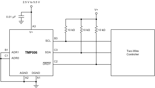
 Figure 19. Typical Application Circuit
9.2.1.1 Design Requirements
For this application, the system must operate over the environment described in Table 8.
Table 8. Wide-Range Parameters
| DESIGN PARAMETER | EXAMPLE VALUE | COMMENT |
|---|---|---|
| N | 32 | Number of devices in calibration set |
| Minimum TDIE | 0°C | Minimum expected die temperature |
| Maximum TDIE | 60°C | Maximum expected die temperature |
| Minimum TOBJ | 0°C | Minimum expected objected temperature |
| Maximum TOBJ | 60°C | Maximum expected object temperature |
| ε | 0.95 | Object emissivity |
| Field of view | 110° | Field of view subtended by object |
| Conversion rate | 1 sample/second |
Select a set of values for TDIE and TOBJ to generate the calibration set. At a minimum, include the four extreme points of the temperature ranges desired. In practice, it is best to include a number of intermediate points as well. This example uses the values shown in Table 9, with an X marking the values chosen for measurement.
Table 9. Wide-Range Measurement Values
| TOBJ | TDIE | |||
|---|---|---|---|---|
| 0°C | 20°C | 40°C | 60°C | |
| 0°C | X | X | X | X |
| 20°C | X | X | X | X |
| 40°C | X | X | X | X |
| 60°C | X | X | X | X |
9.2.1.2 Detailed Design Procedure
Before attempting to calibrate the system, it is necessary to establish the stability of the system. Noise is a measure of precision, which is the random deviation from the mean of the distribution. For a Gaussian (or normal) distribution, the precision is typically characterized by the standard deviation (sensor noise), σ.
9.2.1.2.1 Wide-Range Calibration
To begin calibration, select an object temperature (TOBJ) and a value for the die temperature (TDIE). With these system temperatures stable, take a statistically significant number of samples of VSensor (results shown in register 00h).
In this example, 64 samples were taken.
To compensate for first order drift in system temperatures, it is often useful to normalize the data set. For this purpose, for each temperature set, the sensor voltage data (given in register 00h) is normalized by first finding the best fit line of the form shown in Equation 9:

The normalized data for each data set is then calculated as shown in Equation 10:

The normalized data, VSensor_norm, is centered on zero mean, and is first-order corrected for long-term drift. The standard deviation for each data set is then calculated to estimate the sensor noise, σ. Verify that the data are limited by white noise and no other effects. For a sensor-noise-limited data set, vSENSOR σ is typically < 1 μV, and preferably < 0.5 μV after first-order correction for drift, as described previously. If this condition is not satisfied, then the calibration accuracy is limited by external system factors (for example, convection or conduction). Repeat this process for each combination of TOBJ and TDIE for which the calibration is to be performed. The normalized data are used only for evaluating the suitability of the data set for calibration, and not for the actual calibration itself.
For calibration, the mean value, <VSENSOR>, is calculated for each combination of TOBJ and TDIE, as shown in Table 10. Using the mean value minimizes error introduced by random noise. Based on the means, a set of coefficients is generated based on a user-selected optimization criteria for Equation 7. Common criteria are minimizing the maximum error, minimizing the average error, and so on. For a detailed discussion of optimization methods, see user guide SBOU142, TMP007 Calibration Guide.
Table 10. Mean Values
| TOBJ | TDIE | |||
|---|---|---|---|---|
| 0°C | 20°C | 40°C | 60°C | |
| 0°C | <VSENSOR> | <VSENSOR> | <VSENSOR> | <VSENSOR> |
| 20°C | <VSENSOR> | <VSENSOR> | <VSENSOR> | <VSENSOR> |
| 40°C | <VSENSOR> | <VSENSOR> | <VSENSOR> | <VSENSOR> |
| 60°C | <VSENSOR> | <VSENSOR> | <VSENSOR> | <VSENSOR> |
9.2.1.2.2 Verifying the Calibration
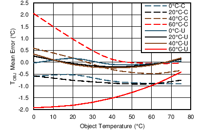
The next step is to use the generated coefficients to verify the calibration, and determine the accuracy of the system. For common calibration (C) , the same coefficients are used for all devices; in unit calibration (U) the coefficients are calculated for each device. Common calibration includes device-to-device variation, and thus is less accurate, but much easier to implement. Unit calibration is more accurate, and eliminates device variation, but requires more effort to implement. The choice depends on the application requirements for accuracy versus implementation effort.
Mean calibration error at each point is defined as shown in Equation 11:

where
- TOBJ_PREDICT is the temperature based on the calibration coefficients.
- TOBJ_ACTUAL is the known object temperature, measured independently.
- N is the number of devices in the calibration set.
The mean error graph (see Figure 20) provides an efficient method of understanding how the systematic errors vary across the temperature ranges of interest. This graph also provides a means of weighing the benefits and efforts of common versus unit calibration for a particular application.
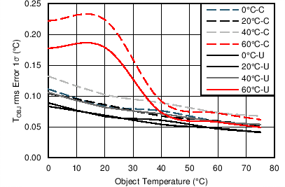
Note that calibration does not affect the temporal random noise observed, as shown in Figure 21. The standard deviation of the temperature error is independent of the calibration if the random error is dominated by the sensor noise and not external system factors, such as convection and conduction. For common calibration, the total standard deviation increases because of the effects of device-to-device variation. This standard deviation is calculated in the usual way, by substituting TOBJ_PREDICT for the mean in the standard deviation formula.
The accuracy is then defined as the mean calibration error plus the random errors from all sources. For this example application, use the criteria shown in Equation 12:

9.2.1.3 Application Curves
 Figure 20. Mean Calibration Error, Wide Range Over TDIE
 Figure 21. Noise in Temperature Measurement, Wide Range Over TDIE
9.3 System Examples
9.3.1 Use of NEP, NETD, and Responsivity in Estimating System Performance
It is often necessary to estimate system performance as part of the design process. A key system parameter is temperature accuracy for a given set of parameters. Table 11 lists example parameters for estimating system performance.
Table 11. Estimating System Performance Parameters
| DESIGN PARAMETER | EXAMPLE VALUE | COMMENT |
|---|---|---|
| Object distance | 10 mm | Distance to object |
| Object diameter | 15 mm | Object size and geometry |
| ε | 0.95 | Object emissivity |
| TDIE | 23°C | Die temperature |
| TOBJ | 30°C | Maximum expected object temperature |
| FOV | 110° | Field of view subtended by object |
| Responsivity (R0) | 10.8 V/W | Responsivity for TDIE = 25°C, θ = 0° |
| Responsivity (R) | 9 V/W | Responsivity for 110° FOV |
| Sensor rms noise | 0.20 µV | RMS sensor noise at TDIE = 25°C |
| NEP | 30 nW | Thermal power equivalent to rms sensor noise |
| Conversion rate | 1 SPS | SPS = samples per second |
The system accuracy is a function of TOBJ, TDIE, ε, and radiation transfer.
The radiation transfer factor is system dependent, and is affected by the object distance and geometry (for example, planar versus curved surfaces, or presence of lenses). For an planar object perpendicular to the detector axis (see Figure 7), the radiation transfer follows the well-known sin2(θ) result. This expression can be used with a radiation transfer function responsivity value of 9 V/W to estimate system performance.
Because of the angular dependence of the TMP006 and TMP006B detector response, a more accurate representation for the same radiative transfer function geometry is shown in Equation 13:

where
- R0 is the responsivity of the detector to a point source at an angle normal to the detector (θ = 0 in Figure 7. R0 has a value of ~10.8 V/W at 25°C.
The responsivity value of 9 V/W is based on a system with a 110° FOV.
Using the device-specific radiation transfer expression and R0, the detector response is shown in Equation 14:

where
- εOBJ is the emissivity of the object (0.95).
- B is the Stefan-Boltzmann constant (5.67 × 10⁻¹² W/cm2 /K4).
- TOBJ is the object temperature (273 K + 30°C).
- TDIE is the detector temperature (273 K + 23°C).
- Adet is the detector active area (1.09 × 10⁻³ cm2)
- θ is the half-angle subtended by the object as viewed from the detector.
- R0 is the responsivity (~10.8 V/W for the specified temperatures).
The value of cos θ is shown in Equation 15:

where
- r is the distance between the detector and the object (10 mm).
- D is the diameter of the object (15 mm).
Differentiating with respect to object temperature, a small change in temperature creates a small change in the measured voltage given by Equation 16:

Substituting values for the parameters yields Equation 17:

The sensor rms noise at TDIE = 25°C is ~0.25 µV; thus, the rms variation in temperature measurement is as shown in Equation 18:

The peak-to-peak noise is approximately six times the rms noise; therefore, estimate an accuracy of approximately ±0.33°C.
This estimate can also be made using the noise-equivalent power (NEP), noting that NEP is the ratio of noise to responsivity, as shown in Equation 19:

Assuming the system is sensor-noise limited, the NEP is ~30 nW at 25°C, as shown in Equation 20:

Again, the peak-to-peak noise is approximately 6X the rms noise; therefore estimate an accuracy of approximately ±0.42°C.
The different results from these two techniques is because of estimated values used for some parameters. The purpose of these techniques is not to obtain exact answers, but rather to quickly estimate the feasibility of a system implementation based on basic system parameters. These examples are intended only as guidelines; the specific values for the parameters depend on the specific system details.