SBOS518E May 2011 – April 2015 TMP006
PRODUCTION DATA.
- 1 Features
- 2 Applications
- 3 Description
- 4 Revision History
- 5 Device Comparison Table
- 6 Pin Configuration and Functions
- 7 Specifications
-
8 Detailed Description
- 8.1 Overview
- 8.2 Functional Block Diagram
- 8.3 Feature Description
- 8.4 Device Functional Modes
- 8.5 Register Maps
- 9 Application and Implementation
- 10Power-Supply Recommendations
- 11Layout
- 12Device and Documentation Support
- 13Mechanical, Packaging, and Orderable Information
Package Options
Mechanical Data (Package|Pins)
- YZF|8
Thermal pad, mechanical data (Package|Pins)
Orderable Information
8 Detailed Description
8.1 Overview
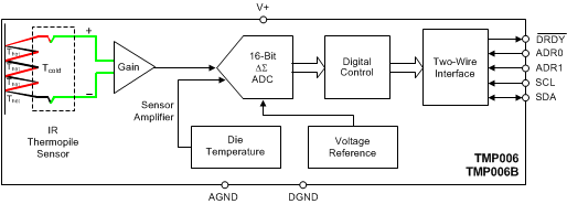
The TMP006 and TMP006B are digital temperature sensors that are optimal for thermal management and thermal protection applications where remote noncontact sensing is desired. The TMP006 and TMP006B use a two-wire interface (I2C and SMBus compatible), and are specified over the die temperature range of –40°C to +125°C. The TMP006 and TMP006B measure object temperatures over a range limited only by the maximum sensor voltage (5.12 mV). The TMP006 and TMP006B contain registers for holding configuration information, temperature measurement results, and sensor voltage measurement. Die temperature and sensor voltage measurements are used to calculate the object temperature.
The TMP006 and TMP006B provide both die temperature and thermopile sensor voltage outputs in a small DSBGA chip-scale package. The die temperature sensor in both the TMP006 and TMP006B is integrated on-chip; the thermal path runs through the DSBGA solder balls. The low thermal resistance of the solder balls provides the thermal path to maintain the chip at the temperature of the die environment.
The top side of the DSBGA package must face the object that is being measured with an unobstructed view in order to accurately measure the temperature. Refer to the user guide TMP006 Layout and Assembly Guidelines (SBOU108) for more details.
8.3 Feature Description
The TMP006 and TMP006B sense the IR radiation emitted by all objects. The spectrum of the radiation depends only on the temperature and is given by Planck’s law, as shown in Equation 1:

where
- h = Planck’s constant
- c = speed of light
- kB = Boltzmann’s constant
- λ = wavelength in microns
The intensity of radiation from the object is determined by the emisivity (ε), a material-dependent property that scales the spectral response so that 0 < ε < 1. For an ideal black body, the radiation is at a maximum for a given temperature and ε = 1. The temperature is measured on the kelvin scale where 0 K is absolute zero, or –273.15°C. Room temperature (25°C) is approximately 298.13 K. The emission spectra for objects at or near room temperature are shown in Figure 5. For these temperatures, the majority of the radiation emitted is in the wavelength range of 3 µm to 20 µm.
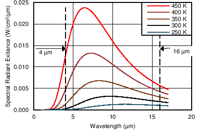 Figure 5. Black Body Emission Spectrum and Response
8.3.1 Spectral Responsivity
The TMP006 and TMP006B are optimized to sense IR radiation emitted by objects from approximately 250 K (–23°C) to 400 K (127°C), with maximum sensitivity from approximately 4 µm to 16 µm. The relative spectral response of the TMP006 and TMP006B is shown in Figure 6.
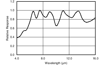 Figure 6. Relative Spectral Response vs Wavelength
8.3.2 Field of View and Angular Response
The TMP006 and TMP006B sense all radiation within a defined field of view (FOV). The FOV (or full-angle of θ) is defined as 2Φ. These devices contain no optical elements, and thus sense all radiation within the hemisphere to the front of the device. Figure 3 shows the angular dependence of the sensor response and the relative power for a circular object that subtends a half angle of phi (Φ). Figure 7 defines the angle Φ in terms of object diameter and distance. Figure 7 assumes that the object is well approximated as a plane that is perpendicular to the sensor axis.
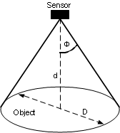 Figure 7. FOV Geometry Definition
In this case, the maximum contribution is from the portion of the object directly in front of the TMP006 or TMP006B (Φ = 0); with the sensitivity per solid angle, dR/dΦ decreases as Φ increases. Approximately 50% of the energy sensed by the TMP006 and TMP006B is within a FOV (θ) = 90°.
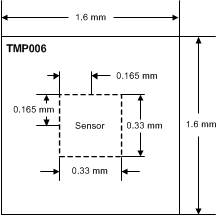
This discussion is for illustrative purposes only; in practice the angular response (dR/dΦ) of the TMP006 and TMP006B to the object is affected by the object orientation, the number of objects, and the precise placement relative to the TMP006 or TMP006B. Figure 8 shows the thermopile sensor dimensions.
8.3.3 Thermopile Principles and Operation
The TMP006 and TMP006B sense radiation by absorbing the radiation on a hot junction. The thermopile then generates a voltage proportional to the temperature difference between the hot junction, Thot, and the cold junction, Tcold.
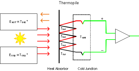 Figure 9. Principle of Thermopile Operation
The cold junction is thermally grounded to the die, and is effectively TDIE, the die temperature. In thermal equilibrium, the hot junction is determined by the object temperature, TOBJ. The energy emitted by the object, EOBJ, minus the energy radiated by the die, EDIE, determines the temperature of the hot junction. The output voltage, VOUT, is therefore determined by the relationship shown in Equation 2:

where
- C is a constant depending on the design of the sensing element.
Note that the sensor voltage is related to both the object temperature and the die temperature. A fundamental characteristic of all thermopiles is that they measure temperature differentials, not absolute temperatures. The TMP006 and TMP006B contain a highly-accurate, internal temperature sensing element to measure TDIE. Estimate TOBJ by using VSENSOR and TDIE. For each 250-ms conversion cycle, the TMP006 and TMP006B measure a value for VSENSOR and for TDIE, which are then placed in their respective registers.
For each conversion cycle, the device generates an analog-to-digital converter (ADC) value for TDIE and VSENSOR. Bits CR2 to CR0 determine the number of TDIE and sensor ADC results to average before they are loaded into the respective registers for readout.
After power-on reset (POR), the TMP006 and TMP006B start in four conversions per second (CR[2:0] = 010). In general, for a mode with N conversions, the local temperature, TDIE, result is updated at the end of the Nth ADC conversion with the value shown in Equation 3:

Similarly, the sensor voltage result is updated at the end of the Nth sensor ADC conversion with the value shown in Equation 4:

The total conversion time and averages per conversion can be optimized to select the best combination of update rate versus noise for an application. Additionally, low-power conversion mode is available. In CR settings 101, 110, and 111, the device inserts a standby time before the beginning of the next conversion or conversions.
The method and requirements for estimating TOBJ are described in the next section.
8.3.4 Object Temperature Calculation
The TMP006 and TMP006B generate a sensor voltage, VSensor, in register 00h that is representative of the energy radiated by the object. In an ideal situation, the Stefan-Boltzman law relates the energy radiated by an object to its temperature by the relationship shown in Equation 5:

where
- σ = Stefan-Boltzman constant = 5.7 × 10⁻¹² W/cm2/K4
- ε = Emissivity, 0 < ε < 1, an object dependent factor, ε = 1 for a perfect black body
A similar relationship holds for the sensing element itself that radiates heat at a rate determined by TDIE. The net energy absorbed by the sensor is then given by the energy absorbed from the object minus the energy radiated by the sensor, as shown in Equation 6:

In an ideal situation, the sensor voltage relates to object temperature as shown in Equation 7:


where
- S is a system-dependent parameter incorporating the object emissivity (ε), FOV, and sensor characteristics. The parameters S0, A1, and A2 are used in determining S.
- f(VOBJ) is a function that compensates for heat flow other than radiation, such as convection and conduction, from nearby objects. The parameters B0, B1, and B2 are used to tune this function to a particular system and environment.
The coefficients affect object temperature measurement as described in Table 1.
Table 1. Calibration Coefficient Definitions
| COEFFICIENT | PURPOSE | CALIBRATION | COMMENT |
|---|---|---|---|
| S0 | FOV and emissivity of object | Application and object dependent | Default values based on black body with ε = 0.95, and 110° FOV |
| A1, A2 | Device properties | Factory set | Default values based on typical sensor characteristics |
| C | Device properties | Factory set | Default values based on typical sensor characteristics |
| B0, B1, B2 | Corrects for energy sources | Environment dependent | Calibrate in end-application environment |
8.3.5 Calibration
The TMP006 and TMP006B default coefficients are calibrated with a black body of emissivity, ε = 0.95, and an FOV (θ) = 110°. Use these coefficients for applications where the object emissivity and geometry satisfy these conditions. For applications with different object emissivity or geometry, calibrate the TMP006 or TMP006B to accurately reflect the object temperature and system geometry. Accuracy is affected by device-to-device or object-to-object variation. For the most demanding applications, calibrate each device individually.
As an overview the calibration procedure includes:
- Defining the environmental variation range (die and object temperature range, supply voltage, temperature change speed, sampling rate and so on).
- Making the die temperature measurements and IR sensor voltage measurements over the environmental range.
- Generate an optimal set of coefficients based on the collected data set.
The best temperature precision is available if every device is calibrated individually. Alternatively, if all the units in the application use the same coefficients, then calibrate a statistically significant number of devices.
Recalibration may be required under any or all of the following conditions:
- Board layout is changed.
- Object or objects in the field of view changed.
- Object distance changed.
- Angle between device surface and direction to the object changed.
- Object and local temperature range changed outside the environmental calibration range.
- Object and local temperature transients significantly changed.
- Supply voltage changed more than 1 V.
- Air convection or conduction near the device.
For further information and methods for calibration, refer to user guide SBOU142, TMP007 Calibration Guide
8.3.6 Sensor Voltage Format
The TMP006 and TMP006B provide 16 bits of data in binary twos complement format. The positive full-scale input produces an output code of 7FFFh and the negative full-scale input produces an output code of 8000h. The output clips at these codes for signals that exceed full-scale. Table 2 summarizes the ideal output codes for different input signals. Figure 10 illustrates code transitions versus input voltage. Full-scale is a 5.12-mV signal. The LSB size is 156.25 nV.
Table 2. Input Signal Versus Ideal Output Code(1)
| SENSOR SIGNAL | OUTPUT CODE |
|---|---|
| FS (215 – 1)/215 (5.12 mV) | 7FFFh |
| +FS/215 (156.25 nV) | 0001h |
| 0 | 0 |
| –FS/215 (–156.25 nV) | FFFFh |
| –FS (–5.12 mV) | 8000h |
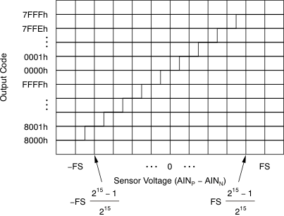 Figure 10. Code Transition Diagram
8.3.7 Temperature Format
The temperature register data format of the TMP006 and TMP006B is reported in a binary twos complement signed integer format, as Table 3 shows, with 1 LSB = 1 / 32°C = 0.03125.
Table 3. Temperature Data Format
| TEMPERATURE (°C) | DIGITAL OUTPUT (BINARY) | SHIFTED HEX |
|---|---|---|
| 150 | 0100 1011 0000 0000 | 12C0 |
| 125 | 0011 1110 1000 0000 | 0FA0 |
| 100 | 0011 0010 0000 0000 | 0C80 |
| 80 | 0010 1000 0000 0000 | 0A00 |
| 75 | 0010 0101 1000 0000 | 0960 |
| 50 | 0001 1001 0000 0000 | 0640 |
| 25 | 0000 1100 1000 0000 | 0320 |
| 0.03125 | 0000 0000 0000 0100 | 0001 |
| 0 | 0000 0000 0000 0000 | 0000 |
| –0.03125 | 1111 1111 1111 1100 | FFFF |
| –0.0625 | 1111 1111 1111 1000 | FFFE |
| –25 | 1111 0011 0111 0000 | FCDC |
| –40 | 1110 1011 1111 1100 | FAFF |
| –55 | 1110 0100 0111 1100 | F91F |
Converting the integer temperature result of the TMP006 and TMP006B to physical temperature is done by right-shifting the last two LSBs followed by a divide-by-32 of TDIE to obtain the physical temperature result in degrees Celsius. TDIE is the 14-bit signed integer contained in the corresponding register. The sign of the temperature is the same as the sign of the integer read from the TMP006 and TMP006B. In twos complement notation, the MSB is the sign bit. If the MSB is 1, the integer is negative and the absolute value can be obtained by inverting all bits and adding 1. An alternative method of calculating the absolute value of negative integers is abs(i) = i xor FFFFh + 1.
8.3.8 Serial Interface
The TMP006 and TMP006B initially start up with typical settings consisting of a conversion rate of one conversion per second (as specified in the Electrical Characteristics). The internal structure of the digital interface is shown in Figure 11.
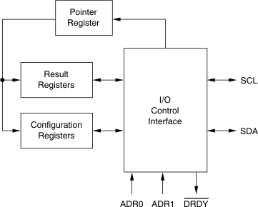 Figure 11. Internal Structure
The TMP006 and TMP006B operate only as a slave device on the two-wire bus. Connections to either bus are made via the open-drain I/O lines, SDA, and SCL. The SDA and SCL pins feature integrated spike-suppression filters and Schmitt triggers to minimize the effects of input spikes and bus noise. The TMP006 and TMP006B support the transmission protocol for fast (1 kHz to 400 kHz) and high-speed (1 kHz to 3.4 MHz) modes. All data bytes are transmitted MSB first.
8.3.8.1 Serial Bus Address
To communicate with the TMP006 or TMP006B, the master must first address slave devices via a slave address byte. The slave address byte consists of seven address bits and a direction bit that indicates the intent to execute a read or write operation.
The TMP006 and TMP006B feature two address pins to allow up to eight devices to be addressed on a single bus. Table 4 describes the pin logic levels used to properly connect up to eight devices. The state of the ADR0 and ADR1 pins is sampled on every bus communication and should be set before any activity on the interface occurs.
8.3.8.2 Read and Write Operations
Access a particular register on the TMP006 and TMP006B by writing the appropriate value to the pointer register. The pointer value is the first byte transferred after the slave address byte with the R/W bit low. Every write operation to the TMP006 and TMP006B requires a value for the pointer (see Figure 12). When reading from the TMP006 or TMP006B, the last value stored in the pointer by a write operation is used to determine which register is read by a read operation. To change the register pointer for a read operation, a new value must be written to the pointer. This transaction is accomplished by issuing a slave address byte with the R/W bit low, followed by the pointer byte. No additional data are required. The master can then generate a START condition and send the slave address byte with the R/W bit high to initiate the read command. If repeated reads from the same register are desired, it is not necessary to continually send the pointer bytes because the TMP006 and TMP006B retain the pointer value until it is changed by the next write operation. Note that register bytes are sent MSB first, followed by the LSB.
8.3.8.3 Two-Wire Timing Diagrams
The TMP006 and TMP006B use a two-wire interface (I2C and SMBus-compatible). Figure 12 and Figure 13 illustrate the timing for the various operations on the TMP006 and TMP006B. Parameters for Figure 12 are defined in Table 5. Bus definitions are given below.
Table 5. Two-Wire Timing Diagram Definitions
| PARAMETER | TEST CONDITIONS | FAST MODE | HIGH-SPEED MODE | UNIT | ||
|---|---|---|---|---|---|---|
| MIN | MAX | MIN | MAX | |||
| fSCL | SCL operating frequency, VS > 1.7 V | 0.001 | 0.4 | 0.001 | 3.4 | MHz |
| fSCL | SCL operating frequency, VS < 1.7 V | 0.001 | 0.4 | 0.001 | 2.75 | MHz |
| tBUF | Bus free time between STOP and START condition | 600 | 160 | ns | ||
| tHDSTA | Hold time after repeated START condition. After this period, the first clock is generated. |
100 | 100 | ns | ||
| tSUSTA | Repeated START condition setup time | 100 | 100 | ns | ||
| tSUSTO | STOP condition setup time | 100 | 100 | ns | ||
| tHDDAT | Data hold time | 0(1) | 0(2) | ns | ||
| tSUDAT | Data setup time | 100 | 10 | ns | ||
| tLOW | SCL clock low period, VS > 1.7 V | 1300 | 160 | ns | ||
| tLOW | SCL clock low period, VS < 1.7 V | 1300 | 200 | ns | ||
| tHIGH | SCL clock high period | 600 | 60 | ns | ||
| tF | Clock/data fall time | 300 | ns | |||
| tR | Clock/data rise time | 300 | 160 | ns | ||
| tR | Clock/data rise time for SCLK ≤ 100 kHz | 1000 | ns | |||
Bus Idle: Both SDA and SCL lines remain high.
Start Data Transfer: A change in the state of the SDA line from high to low while the SCL line is high defines a START condition. Each data transfer is initiated with a START condition.
Stop Data Transfer: A change in the state of the SDA line from low to high while the SCL line is high defines a STOP condition. Each data transfer terminates with a STOP or a repeated START condition.
Data Transfer: The number of data bytes transferred between a START and a STOP condition is not limited and is determined by the master device. The receiver acknowledges the transfer of data.
Acknowledge: Each receiving device, when addressed, is obliged to generate an Acknowledge bit. A device that acknowledges must pull down the SDA line during the Acknowledge clock pulse in such a way that the SDA line is stable low during the high period of the Acknowledge clock pulse. Setup and hold times must be taken into account. On a master receive, data transfer termination can be signaled by the master generating a Not-Acknowledge on the last byte that has been transmitted by the slave.
In order for the two-wire bus to operate at frequencies above 400 kHz, the master device must issue a High-speed mode (Hs-mode) master code (0000100X) as the first byte after a START condition to switch the bus to high-speed operation. The TMP006 and TMP006B do not acknowledge this byte, but switch the input filters on SDA and SCL and the output filter on SDA to operate in Hs-mode, allowing transfers at up to 3.4 MHz. After the Hs-mode master code has been issued, the master transmits a two-wire slave address to initiate a data transfer operation. The bus continues to operate in Hs-mode until a STOP condition occurs on the bus. Upon receiving the STOP condition, the TMP006 and TMP006B switch the input and output filter back to fast-mode operation.
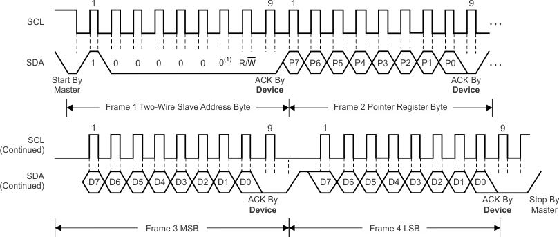
NOINDENT:
Slave address 1000000 shown. Slave address changes for the TMP006 and TMP006B depend on the ADR1 and ADR0 pin connection. See Table 4 for more details.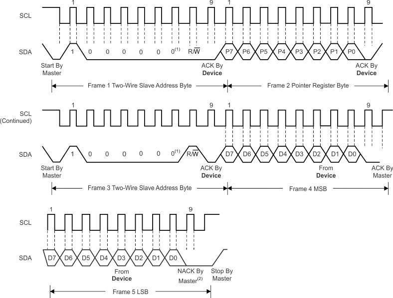
NOINDENT:
Slave address 1000000 shown.NOINDENT:
Master must leave SDA high to terminate a two-byte read operation.8.4 Device Functional Modes
The TMP006 and TMP006B operate in two modes: continuous and shutdown. A software reset function is also available. Selecting the desired operating mode is done by writing to the configuration register conversion mode select bits MOD[2:0]. The duration of the analog-to-digital (A/D) conversion is determined by the conversion rate bits CR[2:0] and is listed in Table 7. Continuous mode, on the other hand, performs an A/D conversion followed by a low-power delay in order to reduce the average power consumption. Multiple options for the conversion time and delay time are available in order to select the desired power and noise performance. Initiating power-down has an immediate effect; it aborts the current conversion and puts the device into a low-power shutdown mode. RST, or software reset, is also immediate and initializes all memory locations with the respective reset values.
8.5 Register Maps
The TMP006 and TMP006B contain data registers that hold configuration information, temperature measurement results, and status information.
Table 6. Register Map
| POINTER (HEX) | REGISTER | D15 | D14 | D13 | D12 | D11 | D10 | D9 | D8 | D7 | D6 | D5 | D4 | D3 | D2 | D1 | D0 |
|---|---|---|---|---|---|---|---|---|---|---|---|---|---|---|---|---|---|
| 00h | Sensor voltage | V15 | V14 | V13 | V12 | V11 | V10 | V9 | V8 | V7 | V6 | V5 | V4 | V3 | V2 | V1 | V0 |
| 01h | Local temperature | T13 | T12 | T11 | T10 | T9 | T8 | T7 | T6 | T5 | T4 | T3 | T2 | T1 | T0 | 0 | 0 |
| 02h | Configuration | RST | MOD3 | MOD2 | MOD1 | CR3 | CR2 | CR1 | EN | DRDY | 0 | 0 | 0 | 0 | 0 | 0 | 0 |
| FEh | Manufacturer ID | ID15 | ID14 | ID13 | ID12 | ID11 | ID10 | ID9 | ID8 | ID7 | ID6 | ID5 | ID4 | ID3 | ID2 | ID1 | ID0 |
| FFh | Device ID | ID15 | ID14 | ID13 | ID12 | ID11 | ID10 | ID9 | ID8 | ID7 | ID6 | ID5 | ID4 | ID3 | ID2 | ID1 | ID0 |
8.5.1 Sensor Voltage Result (VSENSOR) Register (address = 00h) [reset = 0000000000000000]
The sensor voltage register is a 16-bit result register in binary twos complement format. One least significant bit (LSB) is 156.25 nV. The full-scale value is a ±5.12 mV signal. Data from this register (Figure 14) are used in conjunction with data from the Temperature register to calculate the object temperature. Figure 14 summarizes the Sensor Voltage register. The equation for the resultant object temperature is discussed in the TMP006 User Guide (SBOU107).
| 15 | 14 | 13 | 12 | 11 | 10 | 9 | 8 | 7 | 6 | 5 | 4 | 3 | 2 | 1 | 0 |
| V15 | V14 | V13 | V12 | V11 | V10 | V9 | V8 | V7 | V6 | V5 | V4 | V3 | V2 | V1 | V0 |
| R-0h | R-0h | R-0h | R-0h | R-0h | R-0h | R-0h | R-0h | R-0h | R-0h | R-0h | R-0h | R-0h | R-0h | R-0h | R-0h |
| LEGEND: R/W = Read/Write; R = Read only; -n = value after reset |
8.5.2 Temperature (TDIE) Register (address = 01h) [reset = 0000000000000000]
The temperature register of the TMP006 and TMP006B is configured as a 14-bit, read-only register (as shown in Figure 15) that stores the result of the most recent conversion for the die temperature, TDIE. Following power-up or a software reset, the Temperature Register reads 0°C (0000h) until the first conversion is complete.
| 15 | 14 | 13 | 12 | 11 | 10 | 9 | 8 | 7 | 6 | 5 | 4 | 3 | 2 | 1 | 0 |
| T13 | T12 | T11 | T10 | T9 | T8 | T7 | T6 | T5 | T4 | T3 | T2 | T1 | T0 | — | — |
| R-0h | R-0h | R-0h | R-0h | R-0h | R-0h | R-0h | R-0h | R-0h | R-0h | R-0h | R-0h | R-0h | R-0h | R-0h | R-0h |
| LEGEND: R/W = Read/Write; R = Read only; -n = value after reset |
8.5.3 Configuration Register (address = 02h) [reset = 0111010000000000]
Figure 16 describes the configuration register. This register determines the operational modes, conversion rate, DRDY control, initiates a single conversion, performs a software reset, or puts the device into shutdown mode. This register is read/write, and the pointer address is 02h.
| 15 | 14 | 13 | 12 | 11 | 10 | 9 | 8 | 7 | 6 | 5 | 4 | 3 | 2 | 1 | 0 |
| RST | MOD2 | MOD1 | MOD0 | CR2 | CR1 | CR0 | EN | DRDY | — | — | — | — | — | — | — |
| R/W-0h | R/W-1h | R/W-1h | R/W-1h | R/W-0h | R/W-1h | R/W-0h | R/W-0h | R/W-0h | R/W-0h | R/W-0h | R/W-0h | R/W-0h | R/W-0h | R/W-0h | R/W-0h |
| LEGEND: R/W = Read/Write; R = Read only; -n = value after reset |
| Bit [15] | RST: Software reset bit |
| 0 = Normal operation, this bit self clears 1 = Software reset |
|
| Bits [14:12] | MOD[2:0]: Mode of operation |
| 000 = Power-down 111 = Sensor and die continuous conversion (MOD) |
|
| Bits [11:9] | CR[2:0]: ADC conversion rate |
| See Table 7. | |
| Bit [8] | EN: DRDY enable bit |
| 0 = DRDY pin disabled 1 = DRDY pin enabled |
|
| Bit [7] | DRDY: Data ready bit |
| 0 = Conversion in progress 1 = Object voltage and ambient temperature results are ready to read. A temperature or sensor voltage read or a write to the Configuration Register is required to clear the condition. |
|
| Bits [6:0] | Unused [6:0] |
Table 7. Conversion Rate
| CR2 | CR1 | CR0 | CONVERSION RATE (conversions/sec) |
TOTAL NUMBER OF AVERAGED SAMPLES | AVERAGE IQ
(μA) |
PEAK-PEAK NOISE OF THE TOBJ RESULT (°C) |
|---|---|---|---|---|---|---|
| 0 | 0 | 0 | 4 | 1 | 240 | 0.5 |
| 0 | 0 | 1 | 2 | 2 | 240 | 0.35 |
| 0 | 1 | 0 | 1 | 4 | 240 | 0.25 (default) |
| 0 | 1 | 1 | 0.5 | 8 | 240 | 0.18 |
| 1 | 0 | 0 | 0.25 | 16 | 240 | 0.125 |
8.5.4 Manufacturer and Device ID Registers
The TMP006 and TMP006B have two identification registers: manufacturer ID (address FEh) shown in Figure 17, and device ID (address FFh) shown in Figure 18. The manufacturer ID reads 5449h and the device ID is 0067h.
8.5.4.1 Manufacturer ID Register (address = FEh) [reset = 0101010001001001]
| 15 | 14 | 13 | 12 | 11 | 10 | 9 | 8 | 7 | 6 | 5 | 4 | 3 | 2 | 1 | 0 |
| ID15 | ID14 | ID13 | ID12 | ID11 | ID10 | ID9 | ID8 | ID7 | ID6 | ID5 | ID4 | ID3 | ID2 | ID1 | ID0 |
| R-0h | R-1h | R-0h | R-1h | R-0h | R-1h | R-0h | R-0h | R-0h | R-1h | R-0h | R-0h | R-1h | R-0h | R-0h | R-1h |
| LEGEND: R/W = Read/Write; R = Read only; -n = value after reset |
