SPRS377F September 2008 – June 2014 TMS320C6745 , TMS320C6747
PRODUCTION DATA.
- 1TMS320C6745, TMS320C6747 Fixed- and Floating-Point Digital Signal Processor
- 2Revision History
-
3Device Overview
- 3.1 Device Characteristics
- 3.2 Device Compatibility
- 3.3 DSP Subsystem
- 3.4 Memory Map Summary
- 3.5 Pin Assignments
- 3.6
Terminal Functions
- 3.6.1 Device Reset and JTAG
- 3.6.2 High-Frequency Oscillator and PLL
- 3.6.3 Real-Time Clock and 32-kHz Oscillator
- 3.6.4 External Memory Interface A (ASYNC, SDRAM)
- 3.6.5 External Memory Interface B (only SDRAM)
- 3.6.6 Serial Peripheral Interface Modules (SPI0, SPI1)
- 3.6.7 Enhanced Capture/Auxiliary PWM Modules (eCAP0, eCAP1, eCAP2)
- 3.6.8 Enhanced Pulse Width Modulators (eHRPWM0, eHRPWM1, eHRPWM2)
- 3.6.9 Enhanced Quadrature Encoder Pulse Module (eQEP)
- 3.6.10 Boot
- 3.6.11 Universal Asynchronous Receiver/Transmitters (UART0, UART1, UART2)
- 3.6.12 Inter-Integrated Circuit Modules (I2C0, I2C1)
- 3.6.13 Timers
- 3.6.14 Universal Host-Port Interface (UHPI)
- 3.6.15 Multichannel Audio Serial Ports (McASP0, McASP1, McASP2)
- 3.6.16 Universal Serial Bus Modules (USB0, USB1)
- 3.6.17 Ethernet Media Access Controller (EMAC)
- 3.6.18 Multimedia Card/Secure Digital (MMC/SD)
- 3.6.19 Liquid Crystal Display Controller (LCD)
- 3.6.20 General Purpose Input Output (GPIO)
- 3.6.21 Reserved and No Connect
- 3.6.22 Supply and Ground
- 3.6.23 Unused USB0 (USB2.0) and USB1 (USB1.1) Pin Configurations
- 4Device Configuration
-
5Device Operating Conditions
- 5.1 Absolute Maximum Ratings Over Operating Case Temperature Range (Unless Otherwise Noted)
- 5.2 Handling Ratings
- 5.3 Recommended Operating Conditions
- 5.4 Notes on Recommended Power-On Hours (POH)
- 5.5 Electrical Characteristics Over Recommended Ranges of Supply Voltage and Operating Case Temperature (Unless Otherwise Noted)
-
6Peripheral Information and Electrical Specifications
- 6.1 Parameter Information
- 6.2 Recommended Clock and Control Signal Transition Behavior
- 6.3 Power Supplies
- 6.4 Reset
- 6.5 Crystal Oscillator or External Clock Input
- 6.6 Clock PLLs
- 6.7 Interrupts
- 6.8 General-Purpose Input/Output (GPIO)
- 6.9 EDMA
- 6.10 External Memory Interface A (EMIFA)
- 6.11 External Memory Interface B (EMIFB)
- 6.12 Memory Protection Units
- 6.13 MMC / SD / SDIO (MMCSD)
- 6.14 Ethernet Media Access Controller (EMAC)
- 6.15 Management Data Input/Output (MDIO)
- 6.16 Multichannel Audio Serial Ports (McASP0, McASP1, and McASP2)
- 6.17
Serial Peripheral Interface Ports (SPI0, SPI1)
- 6.17.1 SPI Peripheral Registers Description(s)
- 6.17.2
SPI Electrical Data/Timing
- 6.17.2.1
Serial Peripheral Interface (SPI) Timing
- Table 6-54 General Timing Requirements for SPI0 Master Modes
- Table 6-55 General Timing Requirements for SPI0 Slave Modes
- Table 6-56 Additional SPI0 Master Timings, 4-Pin Enable Option
- Table 6-57 Additional SPI0 Master Timings, 4-Pin Chip Select Option
- Table 6-58 Additional SPI0 Master Timings, 5-Pin Option
- Table 6-59 Additional SPI0 Slave Timings, 4-Pin Enable Option
- Table 6-60 Additional SPI0 Slave Timings, 4-Pin Chip Select Option
- Table 6-61 Additional SPI0 Slave Timings, 5-Pin Option
- Table 6-62 General Timing Requirements for SPI1 Master Modes
- Table 6-63 General Timing Requirements for SPI1 Slave Modes
- Table 6-64 Additional SPI1 Master Timings, 4-Pin Enable Option
- Table 6-65 Additional SPI1 Master Timings, 4-Pin Chip Select Option
- Table 6-66 Additional SPI1 Master Timings, 5-Pin Option
- Table 6-67 Additional SPI1 Slave Timings, 4-Pin Enable Option
- Table 6-68 Additional SPI1 Slave Timings, 4-Pin Chip Select Option
- Table 6-69 Additional SPI1 Slave Timings, 5-Pin Option
- 6.17.2.1
Serial Peripheral Interface (SPI) Timing
- 6.18 Enhanced Capture (eCAP) Peripheral
- 6.19 Enhanced Quadrature Encoder (eQEP) Peripheral
- 6.20 Enhanced High-Resolution Pulse-Width Modulator (eHRPWM)
- 6.21 LCD Controller
- 6.22 Timers
- 6.23 Inter-Integrated Circuit Serial Ports (I2C0, I2C1)
- 6.24 Universal Asynchronous Receiver/Transmitter (UART)
- 6.25 USB1 Host Controller Registers (USB1.1 OHCI)
- 6.26 USB0 OTG (USB2.0 OTG)
- 6.27 Host-Port Interface (UHPI)
- 6.28 Power and Sleep Controller (PSC)
- 6.29 Programmable Real-Time Unit Subsystem (PRUSS)
- 6.30 Emulation Logic
- 6.31 IEEE 1149.1 JTAG
- 6.32 Real Time Clock (RTC)
- 7Device and Documentation Support
- 8Mechanical Packaging and Orderable Information
Package Options
Refer to the PDF data sheet for device specific package drawings
Mechanical Data (Package|Pins)
- ZKB|256
Thermal pad, mechanical data (Package|Pins)
Orderable Information
6 Device and Documentation Support
6.1 Device Support
6.1.1 Development Support
TI offers an extensive line of development tools for the TMS320C6745/47 platform, including tools to evaluate the performance of the processors, generate code, develop algorithm implementations, and fully integrate and debug software and hardware modules. The tool's support documentation is electronically available within the Code Composer Studio™ Integrated Development Environment (IDE).
The following products support development of TMS320C6745/47 applications:
Software Development Tools:
Code Composer Studio™ Integrated Development Environment (IDE): including Editor
C/C++/Assembly Code Generation, and Debug plus additional development tools
Scalable, Real-Time Foundation Software (DSP/BIOS™), which provides the basic run-time target software needed to support any application.
Hardware Development Tools:
Extended Development System (XDS™) Emulator
For a complete listing of development-support tools for TMS320C6745/47, visit the Texas Instruments web site on the Worldwide Web at www.ti.com uniform resource locator (URL). For information on pricing and availability, contact the nearest TI field sales office or authorized distributor.
6.1.2 Device and Development-Support Tool Nomenclature
To designate the stages in the product development cycle, TI assigns prefixes to the part numbers of all DSP devices and support tools. Each DSP commercial family member has one of three prefixes: TMX, TMP, or TMS (e.g., TMS320C6745). Texas Instruments recommends two of three possible prefix designators for its support tools: TMDX and TMDS. These prefixes represent evolutionary stages of product development from engineering prototypes (TMX/TMDX) through fully qualified production devices/tools (TMS/TMDS).
Device development evolutionary flow:
-
TMX Experimental device that is not necessarily representative of the final device's electrical specifications.
-
TMP Final silicon die that conforms to the device's electrical specifications but has not completed quality and reliability verification.
-
TMS Fully-qualified production device.
Support tool development evolutionary flow:
-
TMDX Development-support product that has not yet completed Texas Instruments internal qualification testing.
-
TMDS Fully qualified development-support product.
TMX and TMP devices and TMDX development-support tools are shipped against the following disclaimer:
"Developmental product is intended for internal evaluation purposes."
TMS devices and TMDS development-support tools have been characterized fully, and the quality and reliability of the device have been demonstrated fully. TI's standard warranty applies.
Predictions show that prototype devices (TMX or TMP) have a greater failure rate than the standard production devices. Texas Instruments recommends that these devices not be used in any production system because their expected end-use failure rate still is undefined. Only qualified production devices are to be used.
TI nomenclature also includes a suffix with the device family name. This suffix indicates the package type (for example, ZKB), the temperature range (for example, "Blank" is the commercial temperature range), and the device speed range in megahertz (for example, "Blank" is the default).
Figure 6-1 provides a legend for reading the complete device name for any TMS320C674x member.
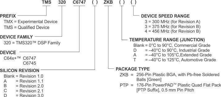 Figure 6-1 Device Nomenclature
6.2 Documentation Support
The following documents describe the TMS320C6745/47 Low-power digital signal processor. Copies of these documents are available on the Internet at www.ti.com. Tip: Enter the literature number in the search box provided at www.ti.com.
-
DSP Reference Guides
-
SPRUFE8 TMS320C674x DSP CPU and Instruction Set Reference Guide. Describes the CPU architecture, pipeline, instruction set, and interrupts for the TMS320C674x digital signal processors (DSPs). The C674x DSP is an enhancement of the C64x+ and C67x+ DSPs with added functionality and an expanded instruction set.
-
SPRUFK5 TMS320C674x DSP Megamodule Reference Guide. Describes the TMS320C674x digital signal processor (DSP) megamodule. Included is a discussion on the internal direct memory access (IDMA) controller, the interrupt controller, the power-down controller, memory protection, bandwidth management, and the memory and cache.
-
SPRUH91TMS320C6745/C6747 DSP Technical Reference Manual. Describes the System-on-Chip (SoC) and each peripheral in the device.
-
User's Guides
-
SPRU186 TMS320C6000 Assembly Language Tools User's Guide.Describes the assembly language tools (assembler, linker, and other tools used to develop assembly language code), assembler directives, macros, common object file format, and symbolic debugging directives for the TMS320C6000 platform of devices (including the C64x+, C67x+, and C674x generations).
-
SPRU187 TMS320C6000 Optimizing Compiler User's Guide. Describes the TMS320C6000 C compiler and the assembly optimizer. This C compiler accepts ANSI standard C source code and produces assembly language source code for the TMS320C6000 platform of devices (including the C64x+, C67x+, and C674x generations). The assembly optimizer helps you optimize your assembly code.
-
SPRUG82 TMS320C674x DSP Cache User's Guide. Explains the fundamentals of memory caches and describes how the two-level cache-based internal memory architecture in the TMS320C674x digital signal processor (DSP) can be efficiently used in DSP applications. Shows how to maintain coherence with external memory, how to use DMA to reduce memory latencies, and how to optimize your code to improve cache efficiency. The internal memory architecture in the C674x DSP is organized in a two-level hierarchy consisting of a dedicated program cache (L1P) and a dedicated data cache (L1D) on the first level. Accesses by the CPU to the these first level caches can complete without CPU pipeline stalls. If the data requested by the CPU is not contained in cache, it is fetched from the next lower memory level, L2 or external memory.
6.3 Community Resources
The following links connect to TI community resources. Linked contents are provided "AS IS" by the respective contributors. They do not constitute TI specifications and do not necessarily reflect TI's views; see TI's Terms of Use.
-
TI E2E™ Online Community TI's Engineer-to-Engineer (E2E) Community. Created to foster collaboration among engineers. At e2e.ti.com, you can ask questions, share knowledge, explore ideas and help solve problems with fellow engineers.
-
TI Embedded Processors Wiki Texas Instruments Embedded Processors Wiki. Established to help developers get started with Embedded Processors from Texas Instruments and to foster innovation and growth of general knowledge about the hardware and software surrounding these devices.
6.4 Related Links
The table below lists quick access links. Categories include technical documents, support and community resources, tools and software, and quick access to sample or buy.
Table 6-1 Related Links
| PARTS | PRODUCT FOLDER | SAMPLE & BUY | TECHNICAL DOCUMENTS | TOOLS & SOFTWARE | SUPPORT & COMMUNITY |
|---|---|---|---|---|---|
| TMS320C6745 | Click here | Click here | Click here | Click here | Click here |
| TMS320C6747 | Click here | Click here | Click here | Click here | Click here |
6.5 Trademarks
DSP/BIOS, PowerPAD, TMS320C6000, C6000, E2E are trademarks of Texas Instruments.
All other trademarks are the property of their respective owners.
6.6 Electrostatic Discharge Caution

This integrated circuit can be damaged by ESD. Texas Instruments recommends that all integrated circuits be handled with appropriate precautions. Failure to observe proper handling and installation procedures can cause damage.
ESD damage can range from subtle performance degradation to complete device failure. Precision integrated circuits may be more susceptible to damage because very small parametric changes could cause the device not to meet its published specifications.
6.7 Glossary
SLYZ022 — TI Glossary.
This glossary lists and explains terms, acronyms, and definitions.