SLASE40D May 2015 – April 2016 TPA3251
PRODUCTION DATA.
- 1 Features
- 2 Applications
- 3 Description
- 4 Revision History
- 5 Device Comparison Table
- 6 Pin Configuration and Functions
-
7 Specifications
- 7.1 Absolute Maximum Ratings
- 7.2 ESD Ratings
- 7.3 Recommended Operating Conditions
- 7.4 Thermal Information
- 7.5 Electrical Characteristics
- 7.6 Audio Characteristics (BTL)
- 7.7 Audio Characteristics (SE)
- 7.8 Audio Characteristics (PBTL)
- 7.9 Typical Characteristics, BTL Configuration
- 7.10 Typical Characteristics, SE Configuration
- 7.11 Typical Characteristics, PBTL Configuration
- 8 Parameter Measurement Information
- 9 Detailed Description
- 10Application and Implementation
- 11Power Supply Recommendations
- 12Layout
- 13Device and Documentation Support
- 14Mechanical, Packaging, and Orderable Information
Package Options
Mechanical Data (Package|Pins)
- DDV|44
Thermal pad, mechanical data (Package|Pins)
- DDV|44
Orderable Information
11 Power Supply Recommendations
11.1 Power Supplies
The TPA3251 device requires two external power supplies for proper operation. A high-voltage supply called PVDD is required to power the output stage of the speaker amplifier and its associated circuitry. Additionally, one mid-voltage power supply for GVDD_X and VDD is required to power the gate-drive and other internal digital and analog portions of the device. The allowable voltage range for both the PVDD and the GVDD_X/VDD supplies are listed in the Recommended Operating Conditions table. Ensure both the PVDD and the GVDD_X/VDD supplies can deliver more current than listed in the Electrical Characteristics table.
11.1.1 VDD Supply
The VDD supply required from the system is used to power several portions of the device. It provides power to internal regulators DVDD and AVDD that are used to power digital and analog sections of the device, respectively. Proper connection, routing, and decoupling techniques are highlighted in the TPA3251 device EVM User's Guide SLVUAG8 (as well as the Application Information section and Layout Examples section) and must be followed as closely as possible for proper operation and performance. Deviation from the guidance offered in the TPA3251 device EVM User's Guide, which followed the same techniques as those shown in the Application Information section, may result in reduced performance, errant functionality, or even damage to the TPA3251 device. Some portions of the device also require a separate power supply which is a lower voltage than the VDD supply. To simplify the power supply requirements for the system, the TPA3251 device includes integrated low-dropout (LDO) linear regulators to create these supplies. These linear regulators are internally connected to the VDD supply and their outputs are presented on AVDD and DVDD pins, providing a connection point for an external bypass capacitors. It is important to note that the linear regulators integrated in the device have only been designed to support the current requirements of the internal circuitry, and should not be used to power any additional external circuitry. Additional loading on these pins could cause the voltage to sag and increase noise injection, which negatively affects the performance and operation of the device.
GVDD_X Supply
The GVDD_X supply required from the system is used to power the gate-drives for the output H-bridges. Proper connection, routing, and decoupling techniques are highlighted in the TPA3251 device EVM User's Guide SLVUAG8 (as well as the Application Information section and Layout Examples section) and must be followed as closely as possible for proper operation and performance. Deviation from the guidance offered in the TPA3251 device EVM User's Guide, which followed the same techniques as those shown in the Application Information section, may result in reduced performance, errant functionality, or even damage to the TPA3251 device.
PVDD Supply
The output stage of the speaker amplifier drives the load using the PVDD supply. This is the power supply which provides the drive current to the load during playback. Proper connection, routing, and decoupling techniques are highlighted in the TPA3251 device EVM User's Guide SLVUAG8 (as well as the Application Information section and Layout Examples section) and must be followed as closely as possible for proper operation and performance. Due the high-voltage switching of the output stage, it is particularly important to properly decouple the output power stages in the manner described in the TPA3251 device EVM User's Guide SLVUAG8. The lack of proper decoupling, like that shown in the EVM User's Guide, can results in voltage spikes which can damage the device, or cause poor audio performance and device shutdown faults.
11.2 Powering Up
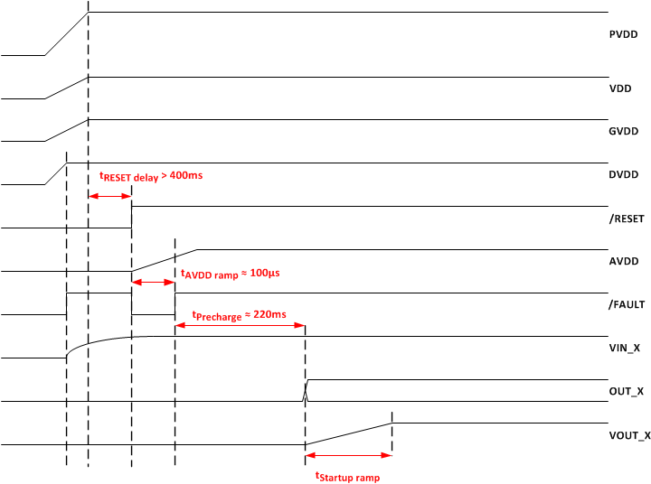
The TPA3251 does not require a power-up sequence, but it is recommended to hold RESET low minimum 400ms after PVDD supply voltage is turned ON. The outputs of the H-bridges remain in a high-impedance state until the gate-drive supply voltage (GVDD_X) and VDD voltage are above the undervoltage protection (UVP) voltage threshold (see the Electrical Characteristics table of this data sheet). This allows an internal circuit to charge the external bootstrap capacitors by enabling a weak pulldown of the half-bridge output as well as initiating a controlled ramp up sequence of the output voltage.
 Figure 28. Startup Timing
When RESET is released to turn on TPA3251, FAULT signal will turn low and AVDD voltage regulator will be enabled. FAULT will stay low until AVDD reaches the undervoltage protection (UVP) voltage threshold (see the Electrical Characteristics table of this data sheet). After a precharge time to stabilize the DC voltage across the input AC coupling capacitors, before the ramp up sequence starts.
11.3 Powering Down
The TPA3251 does not require a power-down sequence. The device remains fully operational as long as the gate-drive supply (GVDD_X) voltage and VDD voltage are above the undervoltage protection (UVP) voltage threshold (see the Electrical Characteristics table of this data sheet). Although not specifically required, it is a good practice to hold RESET low during power down, thus preventing audible artifacts including pops or clicks by initiating a controlled ramp down sequence of the output voltage.