SLOS704B January 2011 – August 2015 TPA6138A2
PRODUCTION DATA.
- 1 Features
- 2 Applications
- 3 Description
- 4 Revision History
- 5 Device Comparison Table
- 6 Pin Configuration and Functions
- 7 Specifications
- 8 Parameter Measurement Information
- 9 Detailed Description
- 10Application and Implementation
- 11Power Supply Recommendations
- 12Layout
- 13Device and Documentation Support
- 14Mechanical, Packaging, and Orderable Information
Package Options
Mechanical Data (Package|Pins)
- PW|14
Thermal pad, mechanical data (Package|Pins)
- PW|14
Orderable Information
9 Detailed Description
9.1 Overview
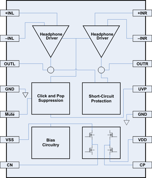
The TPA6138A2 is a DirectPath™ stereo headphone amplifier that requires no output DC blocking capacitors and is capable of delivering 25m-W into a 32-Ω load. The device has built-in pop suppression circuitry to completely eliminate pop noise during turn- on and turn-off. The amplifier outputs have short-circuit protection.
The TPA6138A2 features fully differential inputs to reduce system noise pickup between the audio source and the headphone amplifier. The high power supply noise rejection performance and differential architecture provides increased RF noise immunity.
The TPA6138A2 gain is controlled by external resistors Rin and Rfb, see the Gain-Setting Resistor Ranges section for recommended values.
The TPA6138A2 operates from a single 3-V to 3.6-V supply, as it uses a built-in charge pump to generate a negative voltage supply for the headphone amplifiers.
The TPA6138A2 features an external undervoltage protection which must be set according to TPA6138A2 UVP Operation.
The TPA6138A2 can also be used as a standard operational amplifier (op amp), this makes possible to configure the device as a second-order low-pass filter to remove out-of-band noise.
9.2 Functional Block Diagram

9.3 Feature Description
9.3.1 Direct Path Headphone Driver
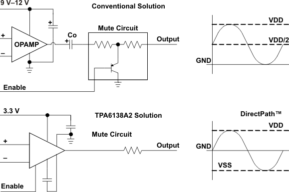
Single-supply line-driver amplifiers typically require dc-blocking capacitors. The top drawing in Figure 7 illustrates the conventional line-driver-amplifier connection to the load and output signal. DC blocking capacitors are often large in value. The headphone load (typical resistive values of 16 Ω to 32 Ω) combine with the dc blocking capacitors to form a high-pass filter. Equation 1 shows the relationship between the load impedance (RL), the capacitor (CO), and the cutoff frequency (fC).

CO can be determined using Equation 2, where the load impedance and the cutoff frequency are known.

If fC is low, the capacitor must then have a large value because the load resistance is small. Large capacitance values require large package sizes. Large package sizes consume PCB area, stand high above the PCB, increase cost of assembly, and can reduce the fidelity of the audio output signal.
 Figure 7. Conventional and DirectPath Line Driver
The DirectPath amplifier architecture operates from a single supply but makes use of an internal charge pump to provide a negative voltage rail. Combining the user-provided positive rail and the negative rail generated by the IC, the device operates in what is effectively a split-supply mode. The output voltages are now centered at zero volts with the capability to swing to the positive rail or negative rail. The DirectPath amplifier requires no output dc-blocking capacitors. The bottom block diagram and waveform of Figure 7 show the ground-referenced line-driver architecture. This is the architecture of the TPA6138A2.
9.4 Device Functional Modes
9.4.1 Mute Operation
The TPA6138A2 is able to turn off the output transistors by asserting to low level the Mute pin. This option is useful when an idle state is needed.
9.4.2 Using the TPA6138A2 as a Second-Order Filter
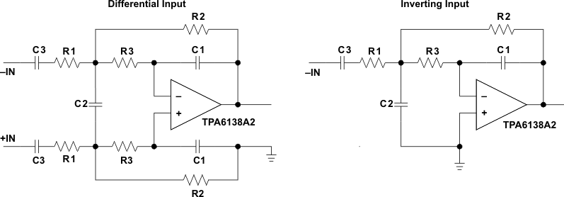
Several audio DACs used today require an external low-pass filter to remove out-of-band noise. This is possible with the TPA6138A2, as it can be used like a standard OPAMP. Several filter topologies can be implemented, both single-ended and differential. In Figure 8, a multi-feedback (MFB) topology with differential input and single-ended input is shown.
An ac-coupling capacitor to remove dc content from the source is shown; it serves to block any dc content from the source and lowers the dc gain to 1, helping to reduce the output dc offset to a minimum.
To calculate the component values, use the TI WEBENCH® Filter Designer (www.ti.com/filterdesigner)
 Figure 8. Second-Order Active Low-Pass Filter
The resistor values should have a low value for obtaining low noise, but should also have a high enough value to allow use of a small-size ac-coupling capacitor. With the proposed values of 15 kΩ, 30 kΩ, and 43 kΩ, a dynamic range (DYR) of 106 dB can be achieved with a 1-μF input ac-coupling capacitor.
9.4.3 TPA6138A2 UVP Operation
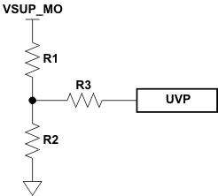
The shutdown threshold at the UVP pin is 1.25 V. The customer must use a resistor divider to obtain the shutdown threshold and hysteresis desired for a particular application. The customer-selected thresholds can be determined as follows:
For example, to obtain VUVP = 3.8 V and 1-V hysteresis, we can use R1 = 3 kΩ, R2 = 1 kΩ and R3 = 50 kΩ.
 Figure 9. UVP Resistor Divider