SLAS997B March 2014 – January 2015 TPA6166A2
PRODUCTION DATA.
- 1 Features
- 2 Applications
- 3 Description
- 4 Revision History
- 5 Pin Configuration and Functions
- 6 Specifications
-
7 Detailed Description
- 7.1 Overview
- 7.2 Functional Block Diagram
- 7.3 Feature Description
- 7.4 Device Functional Modes
- 7.5
Register Maps
- 7.5.1 Register Functional Overview
- 7.5.2 Initialization
- 7.5.3 Typical Use Case Modes
- 7.5.4 Recommended Software Flow Chart
- 7.5.5 Register Map Summary
- 7.5.6
Detailed Register Descriptions
- 7.5.6.1 Register 0x00: Config and Device Status Register 1
- 7.5.6.2 Register 0x01: Config and Device Status Register 2
- 7.5.6.3 Register 0x02: Config and Device Status Register 2
- 7.5.6.4 Register 0x03: Reserved Register
- 7.5.6.5 Register 0x04: Interrupt Mask Register 1
- 7.5.6.6 Register 0x05: Interrupt Mask Register 2
- 7.5.6.7 Register 0x06: Reserved Register
- 7.5.6.8 Register 0x07: Headphone Volume Register 1
- 7.5.6.9 Register 0x08: Headphone Volume Control Register 2
- 7.5.6.10 Register 0x09: Microphone Bias Control Register
- 7.5.6.11 Register 0x0a: Reserved
- 7.5.6.12 Register 0x0b: Revision ID Register
- 7.5.6.13 Register 0x0c: Reserved Register
- 7.5.6.14 Registers 0x0d to 0x10: Reserved Registers
- 7.5.6.15 Register 0x11: Reserved
- 7.5.6.16 Register 0x12: Reserved
- 7.5.6.17 Register 0x13: Reserved
- 7.5.6.18 Register 0x14: Reserved Register
- 7.5.6.19 Register 0x15: Keyscan Debounce Register
- 7.5.6.20 Register 0x16: Keyscan Delay Register
- 7.5.6.21 Register 0x17: Passive Multi Button Keyscan Data Register
- 7.5.6.22 Register 0x18: Jack Detect Test Hardware Settings
- 7.5.6.23 Register 0x19:State Register
- 7.5.6.24 Register 0x1a: Jack Detect Test Hardware Settings
- 7.5.6.25 Registers 0x1b: Reserved
- 7.5.6.26 Register 0x1c: Clock Control
- 7.5.6.27 Register 0x1d: Enable Register 1
- 7.5.6.28 Register 0x1e: Enable Register 2
- 7.5.6.29 Register 0x1F: Reserved
- 7.5.6.30 Register 0x66: Clock Flex Register
- 7.5.6.31 Register 0x6F: Clock Set Register
- 8 Application and Implementation
- 9 Power Supply Recommendations
- 10Layout
- 11Device and Documentation Support
- 12Mechanical, Packaging, and Orderable Information
Package Options
Mechanical Data (Package|Pins)
- YFF|25
Thermal pad, mechanical data (Package|Pins)
Orderable Information
1 Features
- Ultra Low-Power, High-Performance DirectPath™ Class-G Headphone Amplifier
- Ground-Centered Output Eliminates DC-Blocking Capacitors
- 30 mW/Ch into 32 Ω / Ch at 1% THD+N
- –42 dB to +6 dB Volume Control
- 2.0 µV Output Noise at –42 dB Gain
- 91-dB PSRR
- Ground Loop Rejection for Reducing Crosstalk
- Fully Differential Mic Preamplifier With Variable Gain and 3.4-µV Low Noise
- Integrated AC-Coupling Capacitor
- Ground Loop Rejection for Reducing Headphone to Mic Crosstalk
- Choice of Two Mic Bias Voltages: 2.0 V and 2.6 V
- 92-dB PSRR
- Integrated Programmable Mic Bias Resistor
- Advanced Accessory Insertion, Removal, and Type Detection
- Passive Multi-button Support Using 10-Bit SAR ADC
- Implements Proprietary Scheme to Reduce Error Caused by Audio Playback Signal in Presence of Finite Resistance on Headset Ground Return Path
- Integrated Level-4 IEC ESD Protection on Jack Connected Pins (on EVM)
- Ultra Low-Power Chip Shutdown Mode
- I2C Interface
- Short-Circuit Protection
- 0.4-mm Pitch 25-Ball WCSP
2 Applications
- Smart Phones and Wireless Handsets
- Portable Tablets
- Notebook PCs and Docking Stations
3 Description
The TPA6166A2 single-chip headset interface IC simplifies the challenges of detecting what kind of device an end user has plugged into the headphone jack while delivering excellent audio quality. The device enables smaller end products by integrating a high-performance, low-power DirectPath variable-attenuation class-G stereo headphone amplifier, variable-gain microphone preamplifier with bias with advanced accessory detection circuitry, all in a tiny
5-mm × 5-mm terminal, 0.4-mm pitch WCSP package.
The class-G headphone amplifier maximizes battery life by adjusting the supply voltage of the headphone amplifier based on audio signal level. With 8-µV output noise at 0-dB gain and PSRR of 91 dB, the headphone amplifier provides excellent audio performance. DirectPath eliminates the need for DC-blocking capacitors. The microphone preamplifier has two programmable gains of 12 dB and 24 dB, and 3.4 µV input referred noise.
The microphone bias voltage has two programmable settings of 2 V and 2.6 V. The bias output drives up to 1.2 mA of current, has a low output noise of 2 µV, and 92-dB PSRR, providing excellent rejection of power supply noise in wireless handsets.
The advanced accessory detection algorithm automatically detects six supported accessories and enables or disables internal components.
Device Information(1)
| PART NUMBER | PACKAGE | BODY SIZE (NOM) |
|---|---|---|
| TPA6166A2 | WSCP (25) | 2.50 mm × 2.50 mm |
- For all available packages, see the orderable addendum at the end of the data sheet.
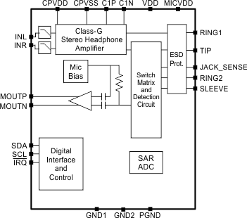
Simplified Schematic
4 Revision History
Changes from A Revision (June 2014) to B Revision
- Added Pin Configuration and Functions section, ESD Ratings table, Feature Description section, Device Functional Modes, Application and Implementation section, Power Supply Recommendations section, Layout section, Device and Documentation Support section, and Mechanical, Packaging, and Orderable Information section Go
Changes from * Revision (January 2014) to A Revision