SLVSDD6B September 2016 – November 2016 TPD8S300
PRODUCTION DATA.
- 1 Features
- 2 Applications
- 3 Description
- 4 Revision History
- 5 Device Comparison Table
- 6 Pin Configuration and Functions
- 7 Specifications
-
8 Detailed Description
- 8.1 Overview
- 8.2 Functional Block Diagram
- 8.3
Feature Description
- 8.3.1 4-Channels of Short-to-VBUS Overvoltage Protection (CC1, CC2, SBU1, SBU2 Pins): 24-VDC Tolerant
- 8.3.2 8-Channels of IEC 61000-4-2 ESD Protection (CC1, CC2, SBU1, SBU2, DP_T, DM_T, DP_B, DM_B Pins)
- 8.3.3 CC1, CC2 Overvoltage Protection FETs 600 mA Capable for Passing VCONN Power
- 8.3.4 CC Dead Battery Resistors Integrated for Handling the Dead Battery Use Case in Mobile Devices
- 8.3.5 3-mm × 3-mm WQFN Package
- 8.4 Device Functional Modes
- 9 Application and Implementation
- 10Power Supply Recommendations
- 11Layout
- 12Device and Documentation Support
- 13Mechanical, Packaging, and Orderable Information
Package Options
Mechanical Data (Package|Pins)
- RUK|20
Thermal pad, mechanical data (Package|Pins)
- RUK|20
Orderable Information
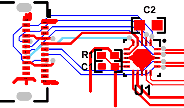
11 Layout
11.1 Layout Guidelines
Proper routing and placement is important to maintain the signal integrity the USB2.0, SBU, CC line signals. The following guidelines apply to the TPD8S300:
- Place the bypass capacitors as close as possible to the VPWR pin, and ESD protection capacitor as close as possible to the VBIAS pin. Capacitors must be attached to a solid ground. This minimizes voltage disturbances during transient events such as short-to-VBUS and ESD strikes.
- The USB2.0 and SBU lines must be routed as straight as possible and any sharp bends must be minimized.
Standard ESD recommendations apply to the C_CC1, C_CC2, C_SBU1, C_SBU2, D1, D2, D3, and D4 pins as well:
- The optimum placement for the device is as close to the connector as possible:
- EMI during an ESD event can couple from the trace being struck to other nearby unprotected traces, resulting in early system failures.
- The PCB designer must minimize the possibility of EMI coupling by keeping any unprotected traces away from the protected traces which are between the TPD8S300 and the connector.
- Route the protected traces as straight as possible.
- Eliminate any sharp corners on the protected traces between the TVS and the connector by using rounded corners with the largest radii possible.
- Electric fields tend to build up on corners, increasing EMI coupling.
- It is best practice to not via up to the D1, D2, D3, and D4 pins from a trace routed on another layer. Rather, it is better to via the trace to the layer with the Dx pin, and to continue that trace on that same layer. See the ESD Protection Layout Guide application report, section 1.3 for more details.
11.2 Layout Example
 Figure 34. TPD8S300 Typical Layout