SLIS125B December 2006 – December 2014 TPIC74100-Q1
PRODUCTION DATA.
- 1 Features
- 2 Applications
- 3 Description
- 4 Revision History
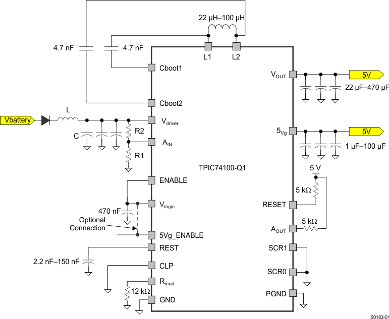
- 5 Pin Configuration and Functions
- 6 Specifications
-
7 Detailed Description
- 7.1 Overview
- 7.2 Functional Block Diagram
- 7.3
Feature Description
- 7.3.1 Switch-Mode Input/Output Pins (L1, L2)
- 7.3.2 Supply Pin (Vdriver)
- 7.3.3 Internal Supply Decoupling Pin (Vlogic)
- 7.3.4 Input Voltage Monitoring Pin (AIN)
- 7.3.5 Input Undervoltage Alarm Pin (AOUT)
- 7.3.6 Reset Delay Timer Pin (REST)
- 7.3.7 Reset Pin (RESET)
- 7.3.8 Main Regulator Output Pin (VOUT)
- 7.3.9 Low-Power-Mode Pin (CLP)
- 7.3.10 Switch-Output Pin (5Vg)
- 7.3.11 5Vg-Enable Pin (5Vg_ENABLE)
- 7.3.12 Slew-Rate Control Pins (SCR0, SCR1)
- 7.3.13 Modulator Frequency Setting (Pin Rmod)
- 7.3.14 Ground Pin (PGND)
- 7.3.15 Enable Pin (ENABLE)
- 7.3.16 Bootstrap Pins (Cboot1 and Cboot2)
- 7.4 Device Functional Modes
- 8 Applications and Implementation
- 9 Power Supply Recommendations
- 10Layout
- 11Device and Documentation Support
- 12Mechanical, Packaging, and Orderable Information
Package Options
Mechanical Data (Package|Pins)
- PWP|20
Thermal pad, mechanical data (Package|Pins)
- PWP|20
Orderable Information
1 Features
- Qualified for Automotive Applications
- AEC-Q100 Qualified With the Following Results:
- Device HBM ESD Classification level 1B for pin 7 (L2), pin 8 (VOUT), pin 9 (5Vg)
- Device HBM ESD Classification 2 for pins 1–6 and 10–20
- Device CDM ESD Classification Level C4B
- Switch-Mode Regulator
- 5 V ±2%, Normal Mode
- 5 V ±3%, Low-Power or Crossover Mode
- Switching Frequency, 440 kHz (typical)
- Input Operating Range, 1.5 V to 40 V, (Vdriver)
- 1-A Load-Current Capability
- 200-mA Load-Current Capability Down to 2-V Input (Vdriver)
- 120-mA Load-Current Capability Down to
1.5-V Input (Vdriver)
- Enable Function
- Low-Power Operation Mode
- Switched 5-V Regulated Output on 5Vg With Current Limit
- Programmable Slew Rate and Frequency Modulation for EMI Consideration
- Reset Function With Deglitch Timer and Programmable Delay
- Alarm Function for Undervoltage Detection and Indication
- Thermally Enhanced Package for Efficient Heat Management
2 Applications
- Automotive Infotainment & Cluster
- Body Electronics
3 Description
The TPIC74100 is a switch-mode regulator with integrated switches for voltage-mode control. With the aid of external components (LC combination), the device regulates the output to 5 V ±3% for a wide input-voltage range.
The TPIC74100 offers a reset function to detect and indicate when the 5-V output rail is outside of the specified tolerance. This reset delay is programmable using an external timing capacitor on the REST pin. Additionally, an alarm (AOUT) feature is activated when the input supply rail Vdriver is below a prescaled specified value (set by the AIN pin).
The TPIC74100 has a frequency-modulation scheme to minimize EMI. The clock modulator permits a modulation of the switching frequency to reduce interference energy in the frequency band.
The 5Vg output is a switched 5-V regulated output with internal current limiting to prevent RESET from being asserted when powering a capacitive load on the supply line. This function is controlled by the 5Vg_ENABLE pin. If there is a short to ground on this output (5Vg output), the output self-protects by operating in a chopping mode. This does, however, increase the output ripple voltage on VOUT during this fault condition.
Device Information(1)
| PART NUMBER | PACKAGE | BODY SIZE (NOM) |
|---|---|---|
| TPIC74100-Q1 | HTSSOP (20) | 6.50 mm x 4.40 mm |
- For all available packages, see the orderable addendum at the end of the datasheet.
Simplified Schematic