SLIS135E December 2010 – February 2017
PRODUCTION DATA.
- 1 Features
- 2 Applications
- 3 Description
- 4 Revision History
- 5 Pin Configuration and Functions
- 6 Specifications
- 7 Detailed Description
- 8 Application and Implementation
- 9 Power Supply Recommendations
- 10Layout
- 11Device and Documentation Support
- 12Mechanical, Packaging, and Orderable Information
Package Options
Mechanical Data (Package|Pins)
- RTE|16
Thermal pad, mechanical data (Package|Pins)
- RTE|16
Orderable Information
8 Application and Implementation
NOTE
Information in the following applications sections is not part of the TI component specification, and TI does not warrant its accuracy or completeness. TI’s customers are responsible for determining suitability of components for their purposes. Customers should validate and test their design implementation to confirm system functionality.
8.1 Application Information
Many applications require using a digital potentiometer such as the TPL0202 for variable resistance or voltage division; the following application shows a few examples. In conjunction with various amplifiers, the TPL0202 can effectively be used in rheostat mode to modify the gain of an amplifier, in voltage divider mode to create a digital-to-analog converter (DAC), or one of the potentiometers can be used in voltage divider mode while the other is in rheostat mode to create a variable current sink.
Digital potentiometers have additional use cases. See the Related Documentation section for additional resources that have application examples including adjustable current source and gain adjustment.
8.2 Typical Application
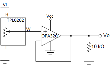
The following typical application shows a DAC.
 Figure 28. DAC Schematic
8.2.1 Design Requirements
Table 3 shows the design parameters for this application.
Table 3. Design Parameters
| DESIGN PARAMETER | EXAMPLE VALUE |
|---|---|
| Input voltage range | 0 to 5 V |
| Output voltage range | 0 to 5 V |
8.2.2 Detailed Design Procedure
The TPL0202 can be used in voltage divider mode with a unity-gain operational amplifier buffer to create an 8-bit DAC. The analog output voltage of the circuit is determined by the wiper setting programmed through the I2C bus.
The operational amplifier is required to buffer the high-impedance output of the TPL0202 or else loading placed on the output of the voltage divider will affect the output voltage.
8.2.3 Application Curve
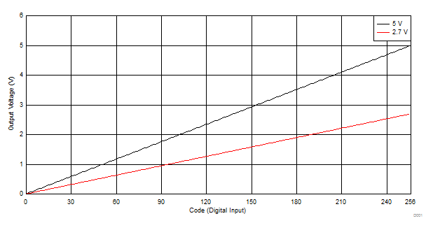
The voltage at terminal H determines the maximum analog voltage at the output. As the TPL0202 moves from zero-scale to full-scale, the voltage divider adjusts with relation to the voltage divider formula (Equation 1), resulting in the desired voltage at terminal W. The voltage at terminal W will range linearly from 0 V to the terminal H voltage. In this example, Vin at terminal H is 5 V and 2.7 V.
 Figure 29. TPL0202 Digital Input vs OPA320 Analog Output (DAC)