SLRS073A May   2017  – May 2018 TPL7407LA

PRODUCTION DATA.  

  1. Features
  2. Applications
  3. Description
    1.     Device Images
      1.      Simple Application Schematic
  4. Revision History
  5. Pin Configuration and Functions
  6. Specifications
    1. 6.1 Absolute Maximum Ratings
    2. 6.2 ESD Ratings
    3. 6.3 Recommended Operating Conditions
    4. 6.4 Thermal Information
    5. 6.5 Electrical Characteristics
    6. 6.6 Switching Characteristics
    7. 6.7 Typical Characteristics
  7. Detailed Description
    1. 7.1 Overview
    2. 7.2 Functional Block Diagram
    3. 7.3 Feature Description
    4. 7.4 Device Functional Modes
      1. 7.4.1 Inductive Load Drive
      2. 7.4.2 Resistive Load Drive
      3. 7.4.3 ON State Input Current
  8. Application and Implementation
    1. 8.1 Application Information
      1. 8.1.1 Unipolar Stepper Motor Driver
      2. 8.1.2 Multi-Purpose Sink Driver
    2. 8.2 Typical Application
      1. 8.2.1 Design Requirements
      2. 8.2.2 Detailed Design Procedure
        1. 8.2.2.1 TTL and other Logic Inputs
        2. 8.2.2.2 Input RC Snubber
        3. 8.2.2.3 High-Impedance Input Drivers
        4. 8.2.2.4 Drive Current
        5. 8.2.2.5 Output Low Voltage
      3. 8.2.3 Application Curve
  9. Power Supply Recommendations
  10. 10Layout
    1. 10.1 Layout Guidelines
    2. 10.2 Layout Example
    3. 10.3 Thermal Considerations
      1. 10.3.1 Improving Package Thermal Performance
  11. 11Device and Documentation Support
    1. 11.1 Receiving Notification of Documentation Updates
    2. 11.2 Community Resources
    3. 11.3 Trademarks
    4. 11.4 Electrostatic Discharge Caution
    5. 11.5 Glossary
  12. 12Mechanical, Packaging, and Orderable Information

Package Options

Mechanical Data (Package|Pins)
Thermal pad, mechanical data (Package|Pins)
Orderable Information

Pin Configuration and Functions

D and PW Package
16-Pin SOIC and TSSOP
Top View
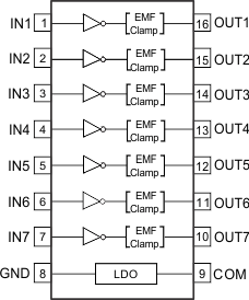
TPL7407LA fun_dia_SLRS073.gif

Pin Functions

PIN I/O DESCRIPTION
NAME NO.
COM 9 Supply pin that must be tied to 6.5 V or higher for proper operation (see the Power Supply Recommendations section for more information)
GND 8 Ground pin
IN(X) 1 I GPIO inputs that drives the outputs "low" (or sink current) when driven "high"
2
3
4
5
6
7
OUT(X) 10 O Driver output that sinks currents after input is driven "high"
11
12
13
14
15
16