SLRS073A May   2017  – May 2018 TPL7407LA

PRODUCTION DATA.  

  1. Features
  2. Applications
  3. Description
    1.     Device Images
      1.      Simple Application Schematic
  4. Revision History
  5. Pin Configuration and Functions
  6. Specifications
    1. 6.1 Absolute Maximum Ratings
    2. 6.2 ESD Ratings
    3. 6.3 Recommended Operating Conditions
    4. 6.4 Thermal Information
    5. 6.5 Electrical Characteristics
    6. 6.6 Switching Characteristics
    7. 6.7 Typical Characteristics
  7. Detailed Description
    1. 7.1 Overview
    2. 7.2 Functional Block Diagram
    3. 7.3 Feature Description
    4. 7.4 Device Functional Modes
      1. 7.4.1 Inductive Load Drive
      2. 7.4.2 Resistive Load Drive
      3. 7.4.3 ON State Input Current
  8. Application and Implementation
    1. 8.1 Application Information
      1. 8.1.1 Unipolar Stepper Motor Driver
      2. 8.1.2 Multi-Purpose Sink Driver
    2. 8.2 Typical Application
      1. 8.2.1 Design Requirements
      2. 8.2.2 Detailed Design Procedure
        1. 8.2.2.1 TTL and other Logic Inputs
        2. 8.2.2.2 Input RC Snubber
        3. 8.2.2.3 High-Impedance Input Drivers
        4. 8.2.2.4 Drive Current
        5. 8.2.2.5 Output Low Voltage
      3. 8.2.3 Application Curve
  9. Power Supply Recommendations
  10. 10Layout
    1. 10.1 Layout Guidelines
    2. 10.2 Layout Example
    3. 10.3 Thermal Considerations
      1. 10.3.1 Improving Package Thermal Performance
  11. 11Device and Documentation Support
    1. 11.1 Receiving Notification of Documentation Updates
    2. 11.2 Community Resources
    3. 11.3 Trademarks
    4. 11.4 Electrostatic Discharge Caution
    5. 11.5 Glossary
  12. 12Mechanical, Packaging, and Orderable Information

Package Options

Mechanical Data (Package|Pins)
Thermal pad, mechanical data (Package|Pins)
Orderable Information

Typical Characteristics

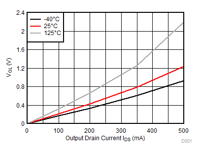
TPL7407LA D001_SLRS073.gif
Figure 1. VOL (VDS)
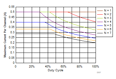
TPL7407LA D007_SLRS066.gif
Figure 3. PW Package Maximum Collector Current vs Duty Cycle at 25°C
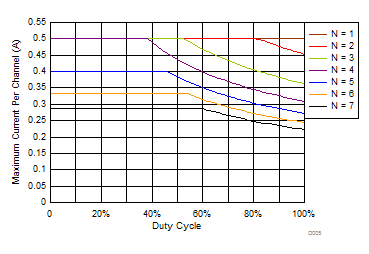
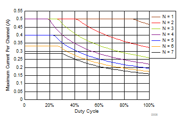
TPL7407LA D005_SLRS066.gif
Figure 5. D Package Maximum Collector Current vs Duty Cycle at 25°C
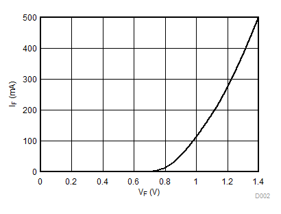
TPL7407LA D002_SLRS073.gif
Figure 2. Flyback Diode Forward Voltage at 25°C
TPL7407LA D008_SLRS066.gif
Figure 4. PW Package Maximum Collector Current vs Duty Cycle at 70°C
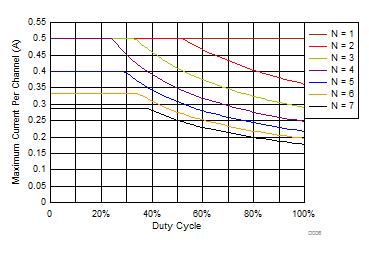
TPL7407LA D006_SLRS066.gif
Figure 6. D Package Maximum Collector Current vs Duty Cycle at 70°C