SLVSB39A December 2011 – June 2014 TPS22929D
PRODUCTION DATA.
- 1 Features
- 2 Applications
- 3 Description
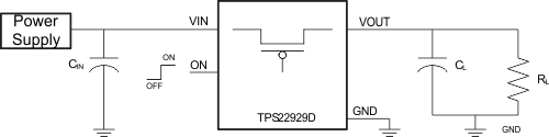
- 4 Simplified Schematic
- 5 Revision History
- 6 Pin Configuration and Functions
- 7 Specifications
- 8 Parametric Measurement Information
- 9 Detailed Description
- 10Application and Implementation
- 11Power Supply Recommendations
- 12Layout
- 13Device and Documentation Support
- 14Mechanical, Packaging, and Orderable Information
Package Options
Mechanical Data (Package|Pins)
- DBV|6
Thermal pad, mechanical data (Package|Pins)
Orderable Information
1 Features
- Integrated Single Load Switch
- Small SOT23-6 Package
- Input Voltage Range: 1.4 V to 5.5 V
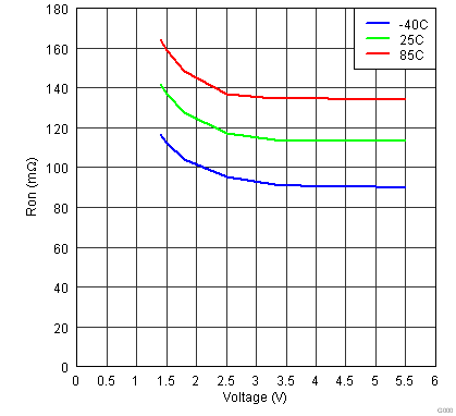
- Low ON-Resistance
- rON = 115 mΩ at VIN = 5 V
- rON = 115 mΩ at VIN = 3.3 V
- rON = 118 mΩ at VIN = 2.5 V
- rON = 129 mΩ at VIN = 1.5 V
- 1.8-A Continuous Switch Current (25°C)
- Low Threshold Control Input
- Controlled Slew-rate
- Under-Voltage Lock Out
- Quick Output Discharge
- Reverse Current Protection
2 Applications
- Portable Industrial Equipment
- Portable Medical Equipment
- Portable Media Players
- Point Of Sales Terminal
- GPS Devices
- Digital Cameras
- Portable Instrumentation
- Smartphones
3 Description
The TPS22929D is a small, low rON load switch with controlled turn on. The device contains a P-channel MOSFET that can operate over an input voltage range of 1.4 V to 5.5 V. The switch is controlled by an on/off input (ON), which is capable of interfacing directly with low-voltage control signals. The TPS22929D is active high enable.
The TPS22929D contains a 150-Ω on-chip load resistor for quick output discharge when the switch is turned off. The rise time of the device is internally controlled in order to avoid inrush current.
The TPS22929D device provides circuit breaker functionality by latching off the power-switch during reverse voltage situations. An internal reverse voltage comparator disables the power-switch when the output voltage (VOUT) is driven higher than the input (VIN) to quickly (10 µs typ) stop the flow of current towards the input side of the switch. Reverse current is always active, even when the power-switch is disabled. Additionally, under-voltage lockout (UVLO) protection turns the switch off if the input voltage is too low.
The TPS22929D is available in a small, space-saving 6-pin SOT23 package and is characterized for operation over the free-air temperature range of –40°C to 85°C.
Device Information(1)
| PART NUMBER | PACKAGE | BODY SIZE (NOM) |
|---|---|---|
| TPS22929D | SOT23 (6) | 2.90 mm × 1.60 mm |
- For all available packages, see the orderable addendum at the end of the datasheet.
4 Simplified Schematic
On-State Resistance vs Input Voltage