SLVSE11A May 2017 – May 2017 TPS2547
PRODUCTION DATA.
- 1 Features
- 2 Applications
- 3 Description
- 4 Revision History
- 5 Pin Configuration and Functions
- 6 Specifications
- 7 Parameter Measurement Information
-
8 Detailed Description
- 8.1 Overview
- 8.2 Functional Block Diagram
- 8.3
Feature Description
- 8.3.1 Standard Downstream Port (SDP) USB 2.0/USB 3.0
- 8.3.2 Charging Downstream Port (CDP)
- 8.3.3 Dedicated Charging Port (DCP)
- 8.3.4 Wake on USB Feature (Mouse/Keyboard Wake Feature)
- 8.3.5 Load Detect
- 8.3.6 Power Wake
- 8.3.7 Port Power Management (PPM)
- 8.3.8 Overcurrent Protection
- 8.3.9 FAULT Response
- 8.3.10 Undervoltage Lockout (UVLO)
- 8.3.11 Thermal Sense
- 8.4 Device Functional Modes
- 9 Application and Implementation
- 10Power Supply Recommendations
- 11Layout
- 12Device and Documentation Support
- 13Mechanical, Packaging, and Orderable Information
Package Options
Mechanical Data (Package|Pins)
- RTE|16
Thermal pad, mechanical data (Package|Pins)
- RTE|16
Orderable Information
1 Features
- D+/D– CDP/DCP Modes per USB BC 1.2
- D+/D– Shorted Mode per Chinese Telecommunication Industry Standard YD/T
1591-2009 - Supports Non-BC1.2 Charging Modes by Automatic Selection:
- D+/D– Divider Modes 2 V/2.7 V and 2.7 V/2 V
- D+/D– 1.2-V Mode
- Supports Sleep-Mode Charging and Mouse/Keyboard Wakeup
- Load Detection for Power Supply Control in S4/S5 Charging and Port Power Management in All Charge Modes
- USB 2.0 and 3.0 Compatible
- Integrated 73-mΩ (Typical) High-Side MOSFET
- 3-A Programmable ILIMIT Supports 15 Watt Loads
- Operating Range: 4.5 V to 5.5 V
- 2 µA/270 µA IQ When Disabled/Enabled
- Drop-In, BOM Compatible with TPS2543/46
- 16-Pin WQFN (3.00 mm × 3.00 mm) Package
- 8-kV ESD Rating on DM/DP Pins
- UL Recognized File No. E169910 and CB Certified - Pending
2 Applications
- USB Ports (Host and Hubs)
- Notebook and Desktop PCs
- Universal Wall-Charging Adapters
3 Description
The TPS2547 is a USB charging port controller and power switch with an integrated USB 2.0 high-speed data line (D+/D–) switch. TPS2547 provides the electrical signatures on D+/D– to support charging schemes listed in Feature Description section. TI tests charging of popular mobile phones, tablets, and media devices with the TPS2547 to ensure compatibility with both BC1.2 compliant, and non-BC1.2 compliant devices.
In addition to charging popular devices, the TPS2547 also supports two distinct power management features, namely, power wake and port power management (PPM) through the STATUS pin. Power wake allows for power supply control in S4/S5 charging and PPM supports intelligent port power management in multiport systems. Additionally, system wake up (from S3) with a mouse/keyboard (both low speed and full speed) is fully supported in the TPS2547.
The TPS2547 73-mΩ power-distribution switch is intended for applications where heavy capacitive loads and short-circuits are likely to be encountered. Two programmable current thresholds provide flexibility for setting current limits and load detect thresholds.
Device Information(1)
| PART NUMBER | PACKAGE | BODY SIZE (NOM) |
|---|---|---|
| TPS2547 | WQFN (16) | 3.00 mm × 3.00 mm |
- For all available packages, see the orderable addendum at the end of the data sheet.
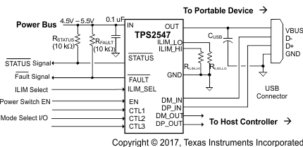
Simplified Schematic
