SLVSDR6C June 2017 – March 2018 TPS25740B
PRODUCTION DATA.
- 1 Features
- 2 Applications
- 3 Description
- 4 Revision History
- 5 Device Comparison Table
- 6 Pin Configuration and Functions
- 7 Specifications
-
8 Detailed Description
- 8.1 Overview
- 8.2 Functional Block Diagram
- 8.3
Feature Description
- 8.3.1 ENSRC
- 8.3.2 USB Type-C CC Logic (CC1, CC2)
- 8.3.3 USB PD BMC Transmission (CC1, CC2, VTX)
- 8.3.4 USB PD BMC Reception (CC1, CC2)
- 8.3.5 Discharging (DSCG, VPWR)
- 8.3.6 Configuring Voltage Capabilities (HIPWR)
- 8.3.7 Configuring Power Capabilities (PSEL, PCTRL, HIPWR)
- 8.3.8 Gate Driver (GDNG, GDNS)
- 8.3.9 Fault Monitoring and Protection
- 8.3.10 Voltage Control (CTL1, CTL2,CTL3)
- 8.3.11 Sink Attachment Indicator (DVDD)
- 8.3.12 Power Supplies (VAUX, VDD, VPWR, DVDD)
- 8.3.13 Grounds (AGND, GND)
- 8.3.14 Output Power Supply (DVDD)
- 8.4 Device Functional Modes
-
9 Application and Implementation
- 9.1
Application Information
- 9.1.1 System-Level ESD Protection
- 9.1.2 Using ENSRC to Enable the Power Supply upon Sink Attachment
- 9.1.3 Use of GD Internal Clamp
- 9.1.4 Resistor Divider on GD for Programmable Start Up
- 9.1.5 Selection of the CTL1, CTL2, and CTL3 Resistors (R(FBL1), R(FBL2), and R(FBL3))
- 9.1.6 Voltage Transition Requirements
- 9.1.7 VBUS Slew Control using GDNG C(SLEW)
- 9.1.8 Tuning OCP using RF and CF
- 9.2 Typical Applications
- 9.3 System Examples
- 9.1
Application Information
- 10Power Supply Recommendations
- 11Layout
- 12Device and Documentation Support
- 13Mechanical, Packaging, and Orderable Information
Package Options
Mechanical Data (Package|Pins)
- RGE|24
Thermal pad, mechanical data (Package|Pins)
- RGE|24
Orderable Information
8.3.5 Discharging (DSCG, VPWR)
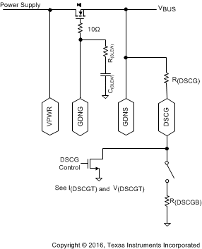
The DSCG pin allows for two different pull-downs that are used to apply different discharging strengths. In addition, the VPWR pin is used to apply a load to discharge the power supply bulk capacitance.
If too much power is dissipated by the device (that is, the TJ1 temperature is exceeded) an OTSD occurs that disables the discharge FET; therefore, an external resistor is recommended in series with the DSCG pin to absorb most of the dissipated power. The external resistor R(DSCG) should be chosen such that the current sunk by the DSCG pin does not exceed I(DSCGT).
The VPWR pin should always be connected to the supply side (as opposed to the connector side) of the power-path switch (Figure 30 shows one example). This pin is monitored before enabling the GDNG gate driver to apply the voltage to the VBUS pin of the connector.
From sink attachment, and while the device has not finalized a USB PD contract, the device applies R(DSCGB).
Also from sink attachment, and while the device has not finalized a USB PD contract, the device draws I(SUPP) through the VPWR pin even if VDD is above its UVLO. This helps to discharge the power supply source.
 Figure 30. Discharge Schematic
The discharge procedure used in the device is intended to allow the DSCG pin to help pull the power supply down from high voltage, and then also pull VBUS at the connector down to the required level (refer to USB PD in Documentation Support).