SLVSDR6C June 2017 – March 2018 TPS25740B
PRODUCTION DATA.
- 1 Features
- 2 Applications
- 3 Description
- 4 Revision History
- 5 Device Comparison Table
- 6 Pin Configuration and Functions
- 7 Specifications
-
8 Detailed Description
- 8.1 Overview
- 8.2 Functional Block Diagram
- 8.3
Feature Description
- 8.3.1 ENSRC
- 8.3.2 USB Type-C CC Logic (CC1, CC2)
- 8.3.3 USB PD BMC Transmission (CC1, CC2, VTX)
- 8.3.4 USB PD BMC Reception (CC1, CC2)
- 8.3.5 Discharging (DSCG, VPWR)
- 8.3.6 Configuring Voltage Capabilities (HIPWR)
- 8.3.7 Configuring Power Capabilities (PSEL, PCTRL, HIPWR)
- 8.3.8 Gate Driver (GDNG, GDNS)
- 8.3.9 Fault Monitoring and Protection
- 8.3.10 Voltage Control (CTL1, CTL2,CTL3)
- 8.3.11 Sink Attachment Indicator (DVDD)
- 8.3.12 Power Supplies (VAUX, VDD, VPWR, DVDD)
- 8.3.13 Grounds (AGND, GND)
- 8.3.14 Output Power Supply (DVDD)
- 8.4 Device Functional Modes
-
9 Application and Implementation
- 9.1
Application Information
- 9.1.1 System-Level ESD Protection
- 9.1.2 Using ENSRC to Enable the Power Supply upon Sink Attachment
- 9.1.3 Use of GD Internal Clamp
- 9.1.4 Resistor Divider on GD for Programmable Start Up
- 9.1.5 Selection of the CTL1, CTL2, and CTL3 Resistors (R(FBL1), R(FBL2), and R(FBL3))
- 9.1.6 Voltage Transition Requirements
- 9.1.7 VBUS Slew Control using GDNG C(SLEW)
- 9.1.8 Tuning OCP using RF and CF
- 9.2 Typical Applications
- 9.3 System Examples
- 9.1
Application Information
- 10Power Supply Recommendations
- 11Layout
- 12Device and Documentation Support
- 13Mechanical, Packaging, and Orderable Information
Package Options
Mechanical Data (Package|Pins)
- RGE|24
Thermal pad, mechanical data (Package|Pins)
- RGE|24
Orderable Information
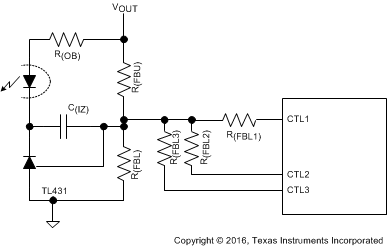
9.1.5 Selection of the CTL1, CTL2, and CTL3 Resistors (R(FBL1), R(FBL2), and R(FBL3))
R(FBL1), R(FBL2), and R(FBL3) provide a means to change the power supply output voltage when switched in by the CTL1, CTL2, and CTL3 open drain outputs, respectively. When CTLx is driven low it will place R(FBLx) in parallel with R(FBL).
 Figure 43. Circuit to Change VOUT Upon Sink/UFP Request
R(FBL2) is calculated using Equation 5. In this example, VOUT9 is 9 V, VOUT15 is 15 V, and VOUT20 is 20 V. VOUT is the default output voltage (5 V) for the regulator and is set by R(FBU), R(FBL) and error amplifier VREF.

R(FBL1) is calculated using Equation 6 after a standard 1% value for R(FBL2) is chosen.


R(FBLx) resistors should be large enough so that the corresponding CTLx sinking current is minimized (< 1 mA). The sinking current for CTLx is VREF / R(FBLx).