SLVSDR6C June 2017 – March 2018 TPS25740B
PRODUCTION DATA.
- 1 Features
- 2 Applications
- 3 Description
- 4 Revision History
- 5 Device Comparison Table
- 6 Pin Configuration and Functions
- 7 Specifications
-
8 Detailed Description
- 8.1 Overview
- 8.2 Functional Block Diagram
- 8.3
Feature Description
- 8.3.1 ENSRC
- 8.3.2 USB Type-C CC Logic (CC1, CC2)
- 8.3.3 USB PD BMC Transmission (CC1, CC2, VTX)
- 8.3.4 USB PD BMC Reception (CC1, CC2)
- 8.3.5 Discharging (DSCG, VPWR)
- 8.3.6 Configuring Voltage Capabilities (HIPWR)
- 8.3.7 Configuring Power Capabilities (PSEL, PCTRL, HIPWR)
- 8.3.8 Gate Driver (GDNG, GDNS)
- 8.3.9 Fault Monitoring and Protection
- 8.3.10 Voltage Control (CTL1, CTL2,CTL3)
- 8.3.11 Sink Attachment Indicator (DVDD)
- 8.3.12 Power Supplies (VAUX, VDD, VPWR, DVDD)
- 8.3.13 Grounds (AGND, GND)
- 8.3.14 Output Power Supply (DVDD)
- 8.4 Device Functional Modes
-
9 Application and Implementation
- 9.1
Application Information
- 9.1.1 System-Level ESD Protection
- 9.1.2 Using ENSRC to Enable the Power Supply upon Sink Attachment
- 9.1.3 Use of GD Internal Clamp
- 9.1.4 Resistor Divider on GD for Programmable Start Up
- 9.1.5 Selection of the CTL1, CTL2, and CTL3 Resistors (R(FBL1), R(FBL2), and R(FBL3))
- 9.1.6 Voltage Transition Requirements
- 9.1.7 VBUS Slew Control using GDNG C(SLEW)
- 9.1.8 Tuning OCP using RF and CF
- 9.2 Typical Applications
- 9.3 System Examples
- 9.1
Application Information
- 10Power Supply Recommendations
- 11Layout
- 12Device and Documentation Support
- 13Mechanical, Packaging, and Orderable Information
Package Options
Mechanical Data (Package|Pins)
- RGE|24
Thermal pad, mechanical data (Package|Pins)
- RGE|24
Orderable Information
9.1.3 Use of GD Internal Clamp
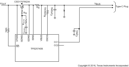
As described in the Configuring Power Capabilities (PSEL, PCTRL, HIPWR) section, the GD pin has an internal clamp. Figure 41 shows an example of how it may be used. VOUT is the voltage from a power supply that is to be provided onto the VBUS wire of the USB Type-C cable through an NFET resistor. If VOUT drops, the NFET should be automatically disabled by the device. This can be accomplished by tying the GD pin to VOUT via a resistor.
The internal resistance of the GD pin is specified to exceed R(GD), and the input threshold is V(GD_TH). The GD pin would therefore draw no more than V(GD_TH) max / R(GD) min< 603 nA. As an example, assume the minimum value of VOUT for which GD should be high is 4.5 V, then the resistor between GD and VOUT may not exceed (4.5 – V(GD_TH) max) / 603e-9 = 4.5 MΩ. To make it robust against board leakage a smaller resistor such as 1 MΩ can be chosen, but the smaller the resistance the more leakage current into the GD pin. In this example, when VOUT is 25 V, the current into the GD pin is (25-V(GDC)) / 1e6 < 1.85 µA.
 Figure 41. Use of GD Internal Clamp