SLVSDR6C June 2017 – March 2018 TPS25740B
PRODUCTION DATA.
- 1 Features
- 2 Applications
- 3 Description
- 4 Revision History
- 5 Device Comparison Table
- 6 Pin Configuration and Functions
- 7 Specifications
-
8 Detailed Description
- 8.1 Overview
- 8.2 Functional Block Diagram
- 8.3
Feature Description
- 8.3.1 ENSRC
- 8.3.2 USB Type-C CC Logic (CC1, CC2)
- 8.3.3 USB PD BMC Transmission (CC1, CC2, VTX)
- 8.3.4 USB PD BMC Reception (CC1, CC2)
- 8.3.5 Discharging (DSCG, VPWR)
- 8.3.6 Configuring Voltage Capabilities (HIPWR)
- 8.3.7 Configuring Power Capabilities (PSEL, PCTRL, HIPWR)
- 8.3.8 Gate Driver (GDNG, GDNS)
- 8.3.9 Fault Monitoring and Protection
- 8.3.10 Voltage Control (CTL1, CTL2,CTL3)
- 8.3.11 Sink Attachment Indicator (DVDD)
- 8.3.12 Power Supplies (VAUX, VDD, VPWR, DVDD)
- 8.3.13 Grounds (AGND, GND)
- 8.3.14 Output Power Supply (DVDD)
- 8.4 Device Functional Modes
-
9 Application and Implementation
- 9.1
Application Information
- 9.1.1 System-Level ESD Protection
- 9.1.2 Using ENSRC to Enable the Power Supply upon Sink Attachment
- 9.1.3 Use of GD Internal Clamp
- 9.1.4 Resistor Divider on GD for Programmable Start Up
- 9.1.5 Selection of the CTL1, CTL2, and CTL3 Resistors (R(FBL1), R(FBL2), and R(FBL3))
- 9.1.6 Voltage Transition Requirements
- 9.1.7 VBUS Slew Control using GDNG C(SLEW)
- 9.1.8 Tuning OCP using RF and CF
- 9.2 Typical Applications
- 9.3 System Examples
- 9.1
Application Information
- 10Power Supply Recommendations
- 11Layout
- 12Device and Documentation Support
- 13Mechanical, Packaging, and Orderable Information
Package Options
Mechanical Data (Package|Pins)
- RGE|24
Thermal pad, mechanical data (Package|Pins)
- RGE|24
Orderable Information
9.1.2 Using ENSRC to Enable the Power Supply upon Sink Attachment
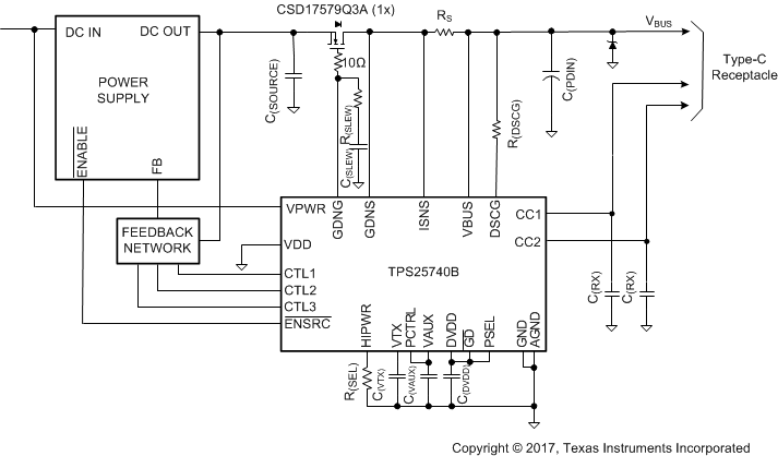
ENSRC may be connected to the enable pin of the power supply as shown in Figure 40. This configuration can eliminate the idle state power loss in the power supply by only turning it on when a sink is attached. In this configuration, VPWR must be connected to a live source so that the TPS25740B can wake upon sink attachment.
 Figure 40. ENSRC as Power Supply Enable
Another benefit of this configuration is that only one NFET is required to block the source capacitance of the power supply when the socket is cold. This requires that the NFET be oriented with drain towards the type C connector as shown in Figure 40. For this NFET orientation, TPS25740B cannot protect the power supply from over-current events, so the power supply must implement over-current protection. For this case, RS may be removed with ISNS directly connected to VBUS. Since VBUS follows DC OUT, power supply start-up overshoot must be less than V(SOVP5). ENSRC is set to high-z after a delay of tHR whenever TPS25740B detects a fault that requires a hard reset.