SLUSA48 June 2016 TPS51200-EP
PRODUCTION DATA.
- 1 Features
- 2 Applications
- 3 Description
- 4 Revision History
- 5 Pin Configuration and Functions
- 6 Specifications
-
7 Detailed Description
- 7.1 Overview
- 7.2 Functional Block Diagram
- 7.3
Feature Description
- 7.3.1 Sink and Source Regulator (VO Pin)
- 7.3.2 Reference Input (REFIN Pin)
- 7.3.3 Reference Output (REFOUT Pin)
- 7.3.4 Soft-Start Sequencing
- 7.3.5 Enable Control (EN Pin)
- 7.3.6 Powergood Function (PGOOD Pin)
- 7.3.7 Current Protection (VO Pin)
- 7.3.8 UVLO Protection (VIN Pin)
- 7.3.9 Thermal Shutdown
- 7.3.10 Tracking Start-up and Shutdown
- 7.4 Device Functional Modes
- 8 Application and Implementation
- 9 Power Supply Recommendations
- 10Layout
- 11Device and Documentation Support
- 12Mechanical, Packaging, and Orderable Information
Package Options
Mechanical Data (Package|Pins)
- DRC|10
Thermal pad, mechanical data (Package|Pins)
- DRC|10
Orderable Information
1 Features
- Input Voltage: Supports 2.5-V Rail and 3.3-V Rail
- VLDOIN Voltage Range: 1.1 V to 3.5 V
- Sink and Source Termination Regulator Includes Droop Compensation
- Requires Minimum Output Capacitance of 20-μF (Typically 3 × 10-μF MLCCs) for Memory Termination Applications (DDR)
- PGOOD to Monitor Output Regulation
- EN Input
- REFIN Input Allows for Flexible Input Tracking Either Directly or Through Resistor Divider
- Remote Sensing (VOSNS)
- ±10-mA Buffered Reference (REFOUT)
- Built-in Soft Start, UVLO, and OCL
- Thermal Shutdown
- Meets DDR and DDR2 JEDEC Specifications
- Supports DDR3, Low-Power DDR3, and DDR4 VTT Applications
- 10-Pin VSON Package With Thermal Pad
-
Supports Defense, Aerospace, and Medical Applications
- Controlled Baseline
- One Assembly and Test Site
- One Fabrication Site
- Available in Military (–55°C to 125°C) Temperature Range
- Extended Product Life Cycle
- Extended Product-Change Notification
- Product Traceability
2 Applications
- Memory Termination Regulator for DDR, DDR2, DDR3, Low-Power DDR3, and DDR4
- Notebooks, Desktops, and Servers
- Telecom and Datacom
- Base Stations
- LCD-TVs and PDP-TVs
- Copiers and Printers
- Set-Top Boxes
3 Description
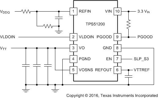
The TPS51200-EP device is a sink and source double data rate (DDR) termination regulator specifically designed for low-input voltage, low-cost, low-noise systems where space is a key consideration.
The TPS51200-EP maintains a fast transient response and only requires a minimum output capacitance of 20 μF. The TPS51200-EP supports a remote sensing function and all power requirements for DDR, DDR2, DDR3, Low-Power DDR3, and DDR4 VTT bus termination.
In addition, the TPS51200-EP provides an open-drain PGOOD signal to monitor the output regulation and an EN signal that can be used to discharge VTT during S3 (suspend to RAM) for DDR applications.
The TPS51200-EP is available in the thermally efficient 10-pin VSON thermal pad package, and is rated both Green and Pb-free. It is specified from –55°C to +125°C.
Device Information(1)
| PART NUMBER | PACKAGE | BODY SIZE (NOM) |
|---|---|---|
| TPS51200-EP | VSON (10) | 3.00 mm × 3.00 mm |
- For all available packages, see the orderable addendum at the end of the data sheet.
Simplified DDR Application
