SLVSB14B October 2011 – February 2016 TPS54821
PRODUCTION DATA.
- 1 Features
- 2 Applications
- 3 Description
- 4 Revision History
- 5 Pin Configuration and Functions
- 6 Specifications
-
7 Detailed Description
- 7.1 Overview
- 7.2 Functional Block Diagram
- 7.3 Feature Description
- 7.4
Device Functional Modes
- 7.4.1 Enable and Adjusting Undervoltage Lockout
- 7.4.2 Adjustable Switching Frequency and Synchronization (RT/CLK)
- 7.4.3 Adjustable Switching Frequency (RT Mode)
- 7.4.4 Synchronization (CLK mode)
- 7.4.5 Slow Start (SS/TR)
- 7.4.6 Power Good (PWRGD)
- 7.4.7 Bootstrap Voltage (BOOT) and Low Dropout Operation
- 7.4.8 Sequencing (SS/TR)
- 7.4.9 Output Overvoltage Protection (OVP)
- 7.4.10 Overcurrent Protection
- 7.4.11 Thermal Shutdown
- 7.4.12 Small Signal Model for Loop Response
- 7.4.13 Simple Small Signal Model for Peak Current Mode Control
- 7.4.14 Small Signal Model for Frequency Compensation
-
8 Application and Implementation
- 8.1 Application Information
- 8.2
Typical Application
- 8.2.1 Design Parameters
- 8.2.2
Design Guide - Step-By-Step Design Procedure
- 8.2.2.1 Typical Application Schematic
- 8.2.2.2 Operating Frequency
- 8.2.2.3 Output Inductor Selection
- 8.2.2.4 Output Capacitor Selection
- 8.2.2.5 Input Capacitor Selection
- 8.2.2.6 Slow Start Capacitor Selection
- 8.2.2.7 Bootstrap Capacitor Selection
- 8.2.2.8 Under Voltage Lockout Set Point
- 8.2.2.9 Output Voltage Feedback Resistor Selection
- 8.2.2.10 Compensation Component Selection
- 8.2.2.11 Fast Transient Considerations
- 8.2.3 Application Curves
- 9 Power Supply Recommendations
- 10Layout
- 11Device and Documentation Support
- 12Mechanical, Packaging, and Orderable Information
Package Options
Mechanical Data (Package|Pins)
- RHL|14
Thermal pad, mechanical data (Package|Pins)
Orderable Information
8 Application and Implementation
NOTE
Information in the following applications sections is not part of the TI component specification, and TI does not warrant its accuracy or completeness. TI’s customers are responsible for determining suitability of components for their purposes. Customers should validate and test their design implementation to confirm system functionality.
8.1 Application Information
The TPS54821 is a highly-integrated, synchronous step-down dc-dc converter. The device is used to convert a higher dc input voltage to a lower dc output voltage with a minimum output current of 8 A.
8.2 Typical Application
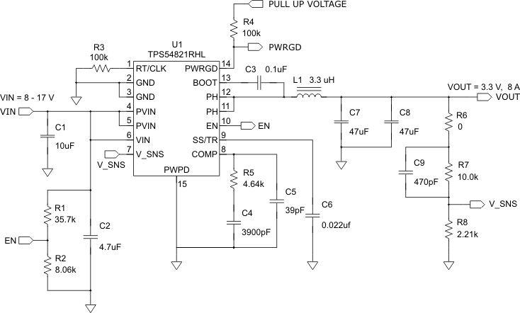 Figure 29. Typical Application Circuit
8.2.1 Design Parameters
This example details the design of a high frequency switching regulator design using ceramic output capacitors. A few parameters must be known in order to start the design process. These parameters are typically determined at the system level. For this example, use the parameters shown in Table 1.
Table 1. Design Parameters
| PARAMETER | VALUE |
|---|---|
| Output Voltage | 3.3 V |
| Output Current | 8 A |
| Transient Response 4 A load step | ΔVout = 7 % |
| Input Voltage | 12 V nominal, 8 V to 17 V |
| Output Voltage Ripple | 33 mV p-p |
| Start Input Voltage (Rising Vin) | 6.528 V |
| Stop Input Voltage (Falling Vin) | 6.193 V |
| Switching Frequency | 480 kHz |
8.2.2 Design Guide – Step-By-Step Design Procedure
8.2.2.1 Typical Application Schematic
The application schematic of Figure 29 was developed to meet the requirements above. This circuit is available as the TPS54821EVM-049 evaluation module. The design procedure is given in this section. For more information about Type II and Type III frequency compensation circuits, see Designing Type III Compensation for Current Mode Step-Down Converters (SLVA352) and Design Calculator (SLVC219).
8.2.2.2 Operating Frequency
The first step is to decide on a switching frequency for the regulator. There is a trade off between higher and lower switching frequencies. Higher switching frequencies may produce smaller a solution size using lower valued inductors and smaller output capacitors compared to a power supply that switches at a lower frequency. However, the higher switching frequency causes extra switching losses, which hurt the converter’s efficiency and thermal performance. In this design, a moderate switching frequency of 480 kHz is selected to achieve both a small solution size and a high efficiency operation.
8.2.2.3 Output Inductor Selection
To calculate the value of the output inductor, use Equation 18. KIND is a coefficient that represents the amount of inductor ripple current relative to the maximum output current. The inductor ripple current is filtered by the output capacitor. Therefore, choosing high inductor ripple currents impact the selection of the output capacitor since the output capacitor must have a ripple current rating equal to or greater than the inductor ripple current. In general, the inductor ripple value is at the discretion of the designer; however, KIND is normally from 0.1 to 0.3 for the majority of applications.

For this design example, use KIND = 0.3 and the minimum inductor value is calculated to be 2.31 µH. For this design, a larger standard value was chosen: 3.3 µH. For the output filter inductor, it is important that the RMS current and saturation current ratings not be exceeded. The RMS and peak inductor current can be found from Equation 20 and Equation 21.


For this design, the RMS inductor current is 8.015 A and the peak inductor current is 8.839 A. The chosen inductor is a Vishay IHLP4040DZER3R3M1series 3.3 µH. It has a saturation current rating of 18.6 A (-20% inductance) and a RMS current rating of 10 A (40°C temperature rise).
The current flowing through the inductor is the inductor ripple current plus the output current. During power up, faults or transient load conditions, the inductor current can increase above the calculated peak inductor current level calculated above. In transient conditions, the inductor current can increase up to the switch current limit of the device. For this reason, the most conservative approach is to specify an inductor with a saturation current rating equal to or greater than the switch current limit rather than the peak inductor current.
8.2.2.4 Output Capacitor Selection
There are three primary considerations for selecting the value of the output capacitor. The output capacitor determines the modulator pole, the output voltage ripple, and how the regulator responds to a large change in load current. The output capacitance needs to be selected based on the more stringent of these three criteria
The desired response to a large change in the load current is the first criteria. The output capacitor needs to supply the load with current when the regulator can not. This situation would occur if there are desired hold-up times for the regulator where the output capacitor must hold the output voltage above a certain level for a specified amount of time after the input power is removed. The regulator is also temporarily not able to supply sufficient output current if there is a large, fast increase in the current needs of the load such as a transition from no load to full load. The regulator usually needs two or more clock cycles for the control loop to see the change in load current and output voltage and adjust the duty cycle to react to the change. The output capacitor must be sized to supply the extra current to the load until the control loop responds to the load change. The output capacitance must be large enough to supply the difference in current for 2 clock cycles while only allowing a tolerable amount of droop in the output voltage. Equation 22 shows the minimum output capacitance necessary to accomplish this.

Where ΔIout is the change in output current, Fsw is the regulators switching frequency and ΔVout is the allowable change in the output voltage. For this example, the transient load response is specified as a 7% change in Vout for a load step of 4 A. For this example, ΔIout = 4 A and ΔVout = 0.07 x 3.3 = 0.231 V. Using these numbers gives a minimum capacitance of 72.2 μF. This value does not take the ESR of the output capacitor into account in the output voltage change. For ceramic capacitors, the ESR is usually small enough to ignore in this calculation.
Equation 23 calculates the minimum output capacitance needed to meet the output voltage ripple specification. Where fsw is the switching frequency, Vripple is the maximum allowable output voltage ripple, and Iripple is the inductor ripple current. In this case, the maximum output voltage ripple is 33mV. Under this requirement, Equation 23 yields 14.6 µF.

Equation 24 calculates the maximum ESR an output capacitor can have to meet the output voltage ripple specification. Equation 24 indicates the ESR should be less than 17.9 mΩ. In this case, the ceramic caps’ ESR is much smaller than 17.9 mΩ.

Additional capacitance de-ratings for aging, temperature and DC bias should be factored in which increases this minimum value. For this example, 2 x 47 μF 10 V X5R ceramic capacitor with 3 mΩ of ESR are used. Capacitors generally have limits to the amount of ripple current they can handle without failing or producing excess heat. An output capacitor that can support the inductor ripple current must be specified. Some capacitor data sheets specify the RMS (Root Mean Square) value of the maximum ripple current. Equation 25 can be used to calculate the RMS ripple current the output capacitor needs to support. For this application, Equation 25 yields 485mA.

8.2.2.5 Input Capacitor Selection
The TPS54821 requires a high quality ceramic, type X5R or X7R, input decoupling capacitor of at least 4.7 µF of effective capacitance on the PVIN input voltage pins and 4.7 µF on the Vin input voltage pin. In some applications additional bulk capacitance may also be required for the PVIN input. The effective capacitance includes any DC bias effects. The voltage rating of the input capacitor must be greater than the maximum input voltage. The capacitor must also have a ripple current rating greater than the maximum input current ripple of the TPS54821. The input ripple current can be calculated using Equation 26.

The value of a ceramic capacitor varies significantly over temperature and the amount of DC bias applied to the capacitor. The capacitance variations due to temperature can be minimized by selecting a dielectric material that is stable over temperature. X5R and X7R ceramic dielectrics are usually selected for power regulator capacitors because they have a high capacitance to volume ratio and are fairly stable over temperature. The output capacitor must also be selected with the DC bias taken into account. The capacitance value of a capacitor decreases as the DC bias across a capacitor increases. For this example design, a ceramic capacitor with at least a 25 V voltage rating is required to support the maximum input voltage. For this example, one 10 μF and one 4.7 µF 25 V capacitors in parallel have been selected as the VIN and PVIN inputs are tied together so the TPS54821 may operate from a single supply. The input capacitance value determines the input ripple voltage of the regulator. The input voltage ripple can be calculated using Equation 27. Using the design example values, Ioutmax = 8 A, Cin = 14.7 μF, Fsw=480 kHz, yields an input voltage ripple of 417 mV and a RMS input ripple current of 3.94 A.

8.2.2.6 Slow Start Capacitor Selection
The slow start capacitor determines the minimum amount of time it takes for the output voltage to reach its nominal programmed value during power up. This is useful if a load requires a controlled voltage slew rate. This is also used if the output capacitance is very large and would require large amounts of current to quickly charge the capacitor to the output voltage level. The large currents necessary to charge the capacitor may make the TPS54821 reach the current limit or excessive current draw from the input power supply may cause the input voltage rail to sag. Limiting the output voltage slew rate solves both of these problems. The soft start capacitor value can be calculated using Equation 28. For the example circuit, the soft start time is not too critical since the output capacitor value is 2 x 47 μF which does not require much current to charge to 3.3 V. The example circuit has the soft start time set to an arbitrary value of 6 ms which requires a 22nF capacitor. In TPS54821, Iss is 2.3µA and Vref is 0.6V.

8.2.2.7 Bootstrap Capacitor Selection
A 0.1 µF ceramic capacitor must be connected between the BOOT to PH pin for proper operation. It is recommended to use a ceramic capacitor with X5R or better grade dielectric. The capacitor should have 10V or higher voltage rating.
8.2.2.8 Under Voltage Lockout Set Point
The Under Voltage Lock Out (UVLO) can be adjusted using the external voltage divider network of R3 and R4. R3 is connected between VIN and the EN pin of the TPS54821 and R4 is connected between EN and GND . The UVLO has two thresholds, one for power up when the input voltage is rising and one for power down or brown outs when the input voltage is falling. For the example design, the supply should turn on and start switching once the input voltage increases above 6.528V (UVLO start or enable). After the regulator starts switching, it should continue to do so until the input voltage falls below 6.190 V (UVLO stop or disable). Equation 2 and Equation 3 can be used to calculate the values for the upper and lower resistor values. For the stop voltages specified the nearest standard resistor value for R3 is 35.7 kΩ and for R4 is 8.06 kΩ.
8.2.2.9 Output Voltage Feedback Resistor Selection
The resistor divider network R7 and R8 is used to set the output voltage. For the example design, 10 kΩ was selected for R7. Using Equation 29, R8 is calculated as 2.22 kΩ. The nearest standard 1% resistor is 2.21 kΩ.

8.2.2.9.1 Minimum Output Voltage
Due to the internal design of the TPS54821, there is a minimum output voltage limit for any given input voltage. The output voltage can never be lower than the internal voltage reference of 0.6 V. Above 0.6 V, the output voltage may be limited by the minimum controllable on time. The minimum output voltage in this case is given by Equation 30

8.2.2.10 Compensation Component Selection
There are several possible methods to design closed loop compensation for dc/dc converters. For the ideal current mode control, the design equations can be easily simplified. The power stage gain is constant at low frequencies, and rolls off at –20 dB/decade above the modulator pole frequency. The power stage phase is 0 degrees at low frequencies and starts to fall one decade above the modulator pole frequency reaching a minimum of –90 degrees one decade above the modulator pole frequency. The modulator pole is a simple pole shown in Equation 31

For the TPS54821 most circuits will have relatively high amounts of slope compensation. As more slope compensation is applied, the power stage characteristics will deviate from the ideal approximations. The phase loss of the power stage will now approach -180 degrees, making compensation more difficult. The power stage transfer function can be solved but it is a tedious hand calculation that does not lend itself to simple approximations. It is best to use Pspice or TINA-TI to accurately model the power stage gain and phase so that a reliable compensation circuit can be designed. That is the technique used in this design procedure. Using the pspice model for the TPS54821, apply the values calculated previously to the output filter components of L1, C7 and C8. Set RLOAD to the appropriate value for the current value to be compensate. For this design, L1 = 3.3 µH. C7 and C8 use the derated capacitance value of 37.6 µF, and the ESR is set to 3 mΩ. The RLOAD resistor is 3.3 V/4 A = 0.82 Ω. Now the power stage characteristic can be plotted as shown in Figure 30.
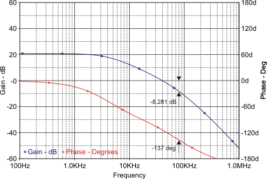 Figure 30. Power Stage Gain and Phase Characteristics
For this design, the intended crossover frequency is 80 kHz. From the power stage gain and phase plots, the gain at 80 kHz is -8.281 dB and the phase is -137 degrees. For 60 degrees of phase margin, additional phase boost from a feed forward capacitor in parallel with the upper resistor of the voltage set point divider will be required. R5 sets the gain of the compensated error amplifier to be equal and opposite the power stage gain at crossover. The required value of R5 can be calculated from Equation 32.

To maximize phase gain, the compensator zero is placed one decade below the crossover frequency of 80 kHz. The required value for C4 is given by Equation 33.

To maximize phase gain the high frequency pole is placed one decade above the crossover frequency of 80 kHz. The required value for C5 can be calculated from Equation 34.

The feed forward capacitor C9, is used to increase the phase boost at crossover above what is normally available from Type II compensation. It places an additional zero/pole pair located at Equation 35 and Equation 36.


This zero and pole pair is not independent. Once the zero location is chosen, the pole is fixed as well. For optimum performance, the zero and pole should be located symmetrically about the intended crossover frequency. The required value for C9 can calculated from Equation 37.

For this design the calculated values for the compensation components are R5 = 4.68 kΩ ,C4 = 4290 pF, C5 = 42.9 pF and C9 = 467 pF. Using standard values, the compensation components are R5 = 4.64 kΩ ,C4 = 3900 pF, C5 = 39 pF and C9 = 470 pF.
8.2.2.11 Fast Transient Considerations
In applications where fast transient responses are important, Type III frequency compensation can be used instead of the traditional Type II frequency compensation.
8.2.3 Application Curves
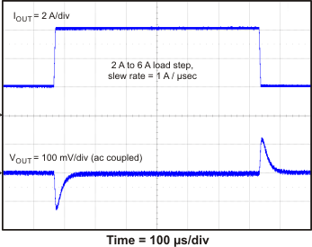 Figure 31. Load Transient
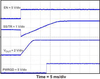 Figure 33. STARTUP with EN
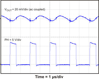 Figure 35. Output Voltage RipplE with Full Load
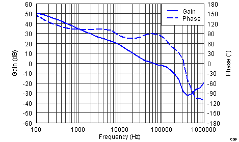 Figure 37. Closed Loop ResponsE, IOUT = 4 A
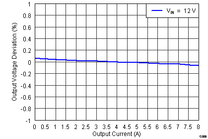 Figure 39. Load Regulation
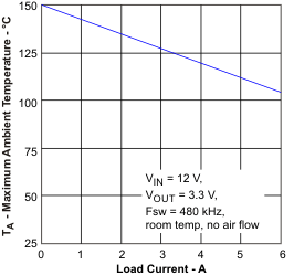 Figure 41. Maximum Ambient Temperature vs Load Current
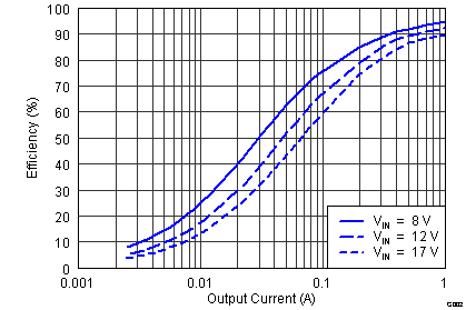 Figure 43. Efficiency vs Output Current
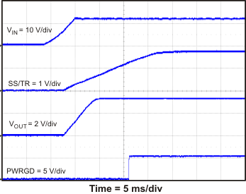 Figure 32. STARTUP with VIN
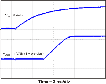 Figure 34. STARTUP with PRE-BIAS
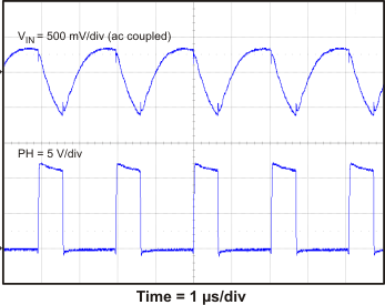 Figure 36. Input Voltage RipplE with Full Load
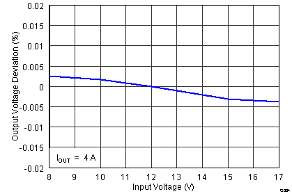 Figure 38. Line Regulation
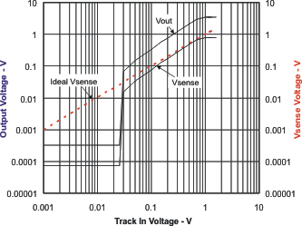 Figure 40. Tracking Performance
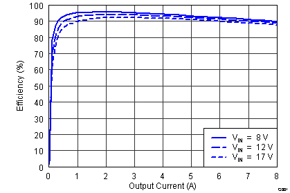 Figure 42. Efficiency vs Load Current
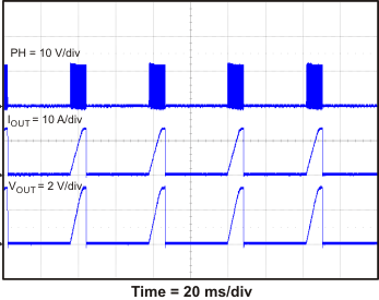 Figure 44. TPS54821 Hiccup Mode Current Limit