SLVSB14B October   2011  – February 2016 TPS54821

PRODUCTION DATA.  

  1. Features
  2. Applications
  3. Description
  4. Revision History
  5. Pin Configuration and Functions
  6. Specifications
    1. 6.1 Absolute Maximum Ratings
    2. 6.2 ESD Ratings
    3. 6.3 Recommended Operating Conditions
    4. 6.4 Thermal Information
    5. 6.5 Electrical Characteristics
    6. 6.6 Typical Characteristics
  7. Detailed Description
    1. 7.1 Overview
    2. 7.2 Functional Block Diagram
    3. 7.3 Feature Description
      1. 7.3.1 Fixed Frequency PWM Control
      2. 7.3.2 Continuous Current Mode Operation (CCM)
      3. 7.3.3 VIN and Power VIN Pins (VIN and PVIN)
      4. 7.3.4 Voltage Reference
      5. 7.3.5 Adjusting the Output Voltage
      6. 7.3.6 Safe Start-up into Pre-Biased Outputs
      7. 7.3.7 Error Amplifier
      8. 7.3.8 Slope Compensation
    4. 7.4 Device Functional Modes
      1. 7.4.1  Enable and Adjusting Undervoltage Lockout
      2. 7.4.2  Adjustable Switching Frequency and Synchronization (RT/CLK)
      3. 7.4.3  Adjustable Switching Frequency (RT Mode)
      4. 7.4.4  Synchronization (CLK mode)
      5. 7.4.5  Slow Start (SS/TR)
      6. 7.4.6  Power Good (PWRGD)
      7. 7.4.7  Bootstrap Voltage (BOOT) and Low Dropout Operation
      8. 7.4.8  Sequencing (SS/TR)
      9. 7.4.9  Output Overvoltage Protection (OVP)
      10. 7.4.10 Overcurrent Protection
      11. 7.4.11 Thermal Shutdown
      12. 7.4.12 Small Signal Model for Loop Response
      13. 7.4.13 Simple Small Signal Model for Peak Current Mode Control
      14. 7.4.14 Small Signal Model for Frequency Compensation
  8. Application and Implementation
    1. 8.1 Application Information
    2. 8.2 Typical Application
      1. 8.2.1 Design Parameters
      2. 8.2.2 Design Guide - Step-By-Step Design Procedure
        1. 8.2.2.1  Typical Application Schematic
        2. 8.2.2.2  Operating Frequency
        3. 8.2.2.3  Output Inductor Selection
        4. 8.2.2.4  Output Capacitor Selection
        5. 8.2.2.5  Input Capacitor Selection
        6. 8.2.2.6  Slow Start Capacitor Selection
        7. 8.2.2.7  Bootstrap Capacitor Selection
        8. 8.2.2.8  Under Voltage Lockout Set Point
        9. 8.2.2.9  Output Voltage Feedback Resistor Selection
          1. 8.2.2.9.1 Minimum Output Voltage
        10. 8.2.2.10 Compensation Component Selection
        11. 8.2.2.11 Fast Transient Considerations
      3. 8.2.3 Application Curves
  9. Power Supply Recommendations
  10. 10Layout
    1. 10.1 PCB Layout Guidelines
    2. 10.2 Layout Example
      1. 10.2.1 Estimated Circuit Area
  11. 11Device and Documentation Support
    1. 11.1 Trademarks
    2. 11.2 Electrostatic Discharge Caution
    3. 11.3 Glossary
  12. 12Mechanical, Packaging, and Orderable Information

Package Options

Mechanical Data (Package|Pins)
Thermal pad, mechanical data (Package|Pins)
Orderable Information

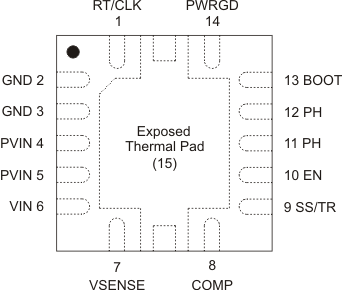
5 Pin Configuration and Functions

RHL Package
14 Pins
(Top View)
TPS54821 po_lvs949.gif

Pin Functions

PIN I/O DESCRIPTION
NAME NO.
RT/CLK 1 I Automatically selects between RT mode and CLK mode. An external timing resistor adjusts the switching frequency of the device; In CLK mode, the device synchronizes to an external clock.
GND 2, 3 - Return for control circuitry and low-side power MOSFET.
PVIN 4, 5 I Power input. Supplies the power switches of the power converter.
VIN 6 I Supplies the control circuitry of the power converter.
VSENSE 7 I Inverting input of the gm error amplifier.
COMP 8 I Error amplifier output, and input to the output switch current comparator. Connect frequency compensation to this pin.
SS/TR 9 I Slow-start and tracking. An external capacitor connected to this pin sets the internal voltage reference rise time. The voltage on this pin overrides the internal reference. It can be used for tracking and sequencing.
EN 10 I Enable pin. Float to enable. Adjust the input undervoltage lockout with two resistors.
PH 11, 12 O The switch node.
BOOT 13 O A bootstrap cap is required between BOOT and PH. The voltage on this cap carries the gate drive voltage for the high-side MOSFET.
PWRGD 14 O Power Good fault pin. Asserts low if output voltage is low due to thermal shutdown, dropout, over-voltage, EN shutdown or during slow start.
Exposed Thermal PAD 15 - Thermal pad of the package and signal ground and it must be soldered down for proper operation.