SLVS441D December 2002 – December 2014 TPS61042
PRODUCTION DATA.
- 1 Features
- 2 Applications
- 3 Description
- 4 Typical Application
- 5 Revision History
- 6 Pin Configuration and Functions
- 7 Specifications
- 8 Detailed Description
- 9 Application and Implementation
- 10Power Supply Recommendations
- 11Layout
- 12Device and Documentation Support
- 13Mechanical, Packaging, and Orderable Information
Package Options
Refer to the PDF data sheet for device specific package drawings
Mechanical Data (Package|Pins)
- DRB|8
Thermal pad, mechanical data (Package|Pins)
- DRB|8
Orderable Information
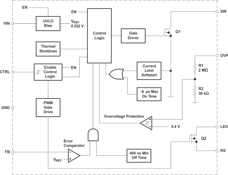
8 Detailed Description
8.1 Overview
The TPS61042 operates like a standard boost converter but regulates the voltage across the sense resistor (RS) instead of the output voltage. This gives an accurate regulated LED current independent of the input voltage and number of LEDs connected. With integrated overvoltage protection (OVP) the TPS61042 is configured as a current source with overvoltage protection ideally suited to drive LEDs. With the 30V internal switch, the device can generate output voltages of up to 27.5 V and has an internal 500mA MOSFET switch (Q1). This allows several LEDs to be connected in series to the output. The internal LED switch (Q2) in series with the LEDs has a maximum current rating of 60 mA and disconnects the LEDs from ground during shutdown. The LED switch is driven by a PWM signal applied to the control pin (CTRL), which directly controls the LED brightness. With this control method the LED brightness depends on the PWM duty cycle only and is independent of the PWM frequency and amplitude.
8.2 Functional Block Diagram
8.3 Feature Description
8.3.1 Boost Converter
The boost converter operates in a pulse frequency modulation (PFM) scheme with constant peak current control. This control scheme maintains high efficiency over the entire load current range and with a switching frequency of up to 1 MHz, enables the use of small external components. The converter monitors the sense voltage across RS with the feedback pin (FB) and, when the feedback voltage falls below the reference voltage (252 mV typ), the main switch turns on and the current ramps up. The main switch turns off when the inductor current reaches the internally set peak current of 500 mA (typ). Refer to the peak current control section for more information. The second criteria that turns off the main switch is the maximum on-time of 6 µs (typ). This limits the maximum on-time of the converter in extreme conditions. As the switch is turned off the external Schottky diode is forward biased, delivering the stored inductor energy to the output. The main switch remains off until the minimum off time of 400 ns (typ) has passed and the feedback voltage is below the reference voltage again. Using this PFM peak current control scheme, the converter operates in discontinuous conduction mode (DCM) where the switching frequency depends on the inductor, input and output voltage, and LED current. Lower LED currents reduce the switching frequency, which results in high efficiency over the entire LED current range. This regulation scheme is inherently stable, allowing a wide range for the selection of the inductor and output capacitor.
8.3.2 Peak Current Control (Boost Converter)
The internal switch is turned on until the inductor current reaches the DC current limit (ILIM) of 500 mA (typ). Due to the internal current limit delay of 100 ns (typ) the actual current exceeds the DC current limit threshold by a small amount. The typical peak current limit can be calculated:


The higher the input voltage and the lower the inductor value, the greater the current limit overshoot.
8.3.3 Softstart
All inductive step-up converters exhibit high in-rush current during start-up if no special precautions are taken. This can cause voltage drops at the input rail during start-up, which may result in an unwanted or premature system shutdown.
The TPS61042 limits this in-rush current during start-up by increasing the current limit in two steps starting from ILIM/4 for 256 switch cycles to ILIM/2 for the next 256 switch cycles and then full current limit. See Figure 23 for typical start-up behavior.
8.3.4 Control (CTRL)
The CTRL pin serves two functions. One is the enable and disable of the device. The other is the PWM control of the internal LED switch (Q2). If no PWM signal is applied to the CTRL pin, then the CTRL pin can be used as a standard enable pin for the device. To enable the device, the CTRL pin must be pulled high for time period of at least 50 µs. The device starts with the Softstart cycle. Pulling the CTRL pin to GND for a time period ≥32 ms disables the device, disconnecting the LEDs from GND by opening the LED switch (Q2) to avoid any LED leakage current. See Figure 11 for the CTRL pin timing.
The internal LED switch (Q2) is driven by the PWM signal when applied to the CTRL pin. Applying a PWM signal in the range of 100 Hz to 50 kHz allows the LED current to be pulsed with the duty cycle of the PWM signal. The CTRL pin accepts a PWM duty cycle from D = 1% to 100%. Duty cycles below 1% are also possible with the restriction that the device is forced into shutdown as the off time of the applied PWM signal exceeds 10 ms.
When a PWM signal is applied to the CTRL pin the LED switch (Q2) turns on immediately. The internal error comparator is disabled for 400 ns. This 400 ns delay time is required to establish the correct voltage level across the sense resistor RS after the LED switch (Q2) is closed.
To achieve good LED current accuracy and linearity, the switching frequency of the converter must be higher than the PWM frequency applied to the CTRL pin.
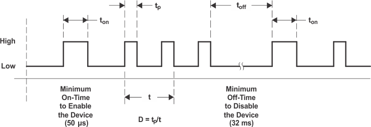 Figure 11. CTRL Timing Diagram
The CTRL timing diagram is shown in Figure 11. To enable the device, the CTRL signal must be high for 50 µs. The PWM signal can then be applied with a pulse width (tp) greater or smaller than tON. To force the device into shutdown mode, the CTRL signal must be low for at least 32 ms. Requiring the CTRL pin to be low for 32mS before the device enters shutdown allows for PWM dimming frequencies as low as 100 Hz. The device is enabled again when a CTRL signal is high for a period of 50 µs minimum. See Figure 10 for the PWM duty cycle versus LED current characteristic.
This CTRL pin must be terminated.
8.3.5 Applying a PWM Signal to the CTRL Pin with an On-Time tp≤2.5µs
In such a case the on-time of the PWM signal, tp, must be >2.5μs until the softstart is completed. The softstart is completed after 512 switching cycles. To simply, estimate the softstart time, multiply the period of the PWM signal times 512, and add 50μs to it. For a 50-kHz signal this would be 10.3ms as a minimum softstart time period. After the softstart time is completed the PWM on time can be reduced to tp >400ns.
8.4 Device Functional Modes
8.4.1 Overvoltage Protection (OVP)
As with any current source, the output voltage rises as the output impedance increases or is disconnected. To prevent the output voltage from exceeding the maximum main switch (Q1) voltage rating of 30 V, an overvoltage protection circuit is integrated. When the output voltage exceeds the OVP threshold voltage, (Q1) turns off. The converter switch remains off until the output voltage falls below the OVP threshold voltage. As long as the output voltage is below the OVP threshold the converter continues its normal operation, until the output voltage exceeds the OVP threshold again.
8.4.2 Undervoltage Lockout
An undervoltage lockout feature prevents mis-operation of the device at input voltages below 1.5 V (typ). As long as the input voltage is below the undervoltage threshold the device remains off, with the main MOSFET switch (Q1) and the LED switch (Q2) open.
8.4.3 Thermal Shutdown
An internal thermal shutdown is implemented in the TPS61042 that shuts down the device if the typical junction temperature of 160°C is exceeded. If the device is in thermal shutdown mode, the main MOSFET switch (Q1) and the LED switch (Q2) are open.