SLVSE09A April   2017  – April 2017 TPS61096A

PRODUCTION DATA.  

  1. Features
  2. Applications
  3. Description
  4. Revision History
  5. Pin Configuration and Functions
  6. Specifications
    1. 6.1 ESD Ratings
    2. 6.2 Recommended Operating Conditions
    3. 6.3 Thermal Information
    4. 6.4 Electrical Characteristics
    5. 6.5 Typical Characteristics
  7. Detailed Description
    1. 7.1 Overview
    2. 7.2 Functional Block Diagram
    3. 7.3 Feature Description
      1. 7.3.1 Controller Circuit
      2. 7.3.2 Current Limit Selection
    4. 7.4 Device Functional Modes
      1. 7.4.1 Under-Voltage Lockout
      2. 7.4.2 Enable and Disable
      3. 7.4.3 Soft Start
      4. 7.4.4 Level Shifters
      5. 7.4.5 Over-voltage Protection
      6. 7.4.6 Thermal Shutdown
  8. Application and Implementation
    1. 8.1 Application Information
    2. 8.2 Typical Application
      1. 8.2.1 Design Requirements
      2. 8.2.2 Detailed Design Procedure
        1. 8.2.2.1 Custom Design With WEBENCH® Tools
        2. 8.2.2.2 Programming the Output Voltage
        3. 8.2.2.3 Maximum Output Current
        4. 8.2.2.4 Inductor Selection
        5. 8.2.2.5 Capacitor Selection
      3. 8.2.3 Application Curves
  9. Power Supply Recommendations
  10. 10Layout
    1. 10.1 Layout Guidelines
    2. 10.2 Layout Example
  11. 11Device and Documentation Support
    1. 11.1 Device Support
      1. 11.1.1 Third-Party Products Disclaimer
      2. 11.1.2 Development Support
        1. 11.1.2.1 Custom Design With WEBENCH® Tools
    2. 11.2 Receiving Notification of Documentation Updates
    3. 11.3 Community Resources
    4. 11.4 Trademarks
    5. 11.5 Electrostatic Discharge Caution
    6. 11.6 Glossary
  12. 12Mechanical, Packaging, and Orderable Information

Package Options

Mechanical Data (Package|Pins)
Thermal pad, mechanical data (Package|Pins)
Orderable Information

Layout

Layout Guidelines

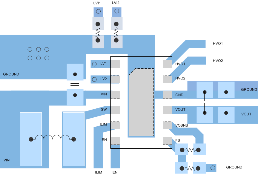
As for all switching power supplies, the layout is an important step in the design, especially at high peak current and high switching frequency. If the layout is not carefully done, the regulator could show stability problems as well as EMI problems. Therefore, use wide and short traces for the main current path and for the power ground paths. The input and output capacitor, as well as inductor should be placed as close as possible to the IC.

Layout Example

A large ground plane on the bottom layer connects the ground pins of the components on the top layer through vias.
TPS61096A figure_20_layout_slvsdb2.gif Figure 23. Example PCB Layout