SLVSE09A April 2017 – April 2017 TPS61096A
PRODUCTION DATA.
- 1 Features
- 2 Applications
- 3 Description
- 4 Revision History
- 5 Pin Configuration and Functions
- 6 Specifications
- 7 Detailed Description
- 8 Application and Implementation
- 9 Power Supply Recommendations
- 10Layout
- 11Device and Documentation Support
- 12Mechanical, Packaging, and Orderable Information
Package Options
Mechanical Data (Package|Pins)
- DSS|12
Thermal pad, mechanical data (Package|Pins)
- DSS|12
Orderable Information
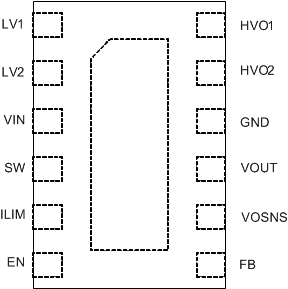
5 Pin Configuration and Functions
DSS Package
12-Pin WSON, 3 mm × 2 mm × 0.75 mm
Top View

Pin Functions
| PIN | TYPE | DESCRIPTION | |
|---|---|---|---|
| NAME | NO. | ||
| LVI1 | 1 | I | Input of level shifter 1 |
| LVI2 | 2 | I | Input of level shifter 2 |
| VIN | 3 | I | IC power supply input |
| SW | 4 | PWR | Switch pin of the converter. It is connected to inductor. |
| ILIM | 5 | I | Inductor peak current limit selection pin. Logic low voltage to select 250mA peak current limit, logic high voltage to select 500mA peak current limit. Must be actively tied high or low. Do not leave it floating. |
| EN | 6 | I | Enable logic input. Logic high voltage enables the device, logic low voltage disables the device. Must be actively tied high or low. Do not leave it floating. |
| FB | 7 | I | Voltage feedback of adjustable output voltage. Connect to the center tap of a resistor divider to program the output voltage. |
| VOSNS | 8 | I/O | Boost converter output voltage sense pin. Connect an external resistor divider between this pin and FB pin. |
| VOUT | 9 | PWR | Boost converter output |
| GND | 10 | PWR | Ground pin |
| HVO2 | 11 | O | Output of level shifter 2 |
| HVO1 | 12 | O | Output of level shifter 1 |