SNVSA79 March 2015 TPS61196-Q1
PRODUCTION DATA.
- 1 Features
- 2 Applications
- 3 Description
- 4 Revision History
- 5 Pin Configuration and Functions
- 6 Specifications
-
7 Detailed Description
- 7.1 Overview
- 7.2 Functional Block Diagram
- 7.3 Feature Description
- 7.4
Device Functional Modes
- 7.4.1
Protections
- 7.4.1.1 Switch Current Limit Protection Using the ISNS Pin
- 7.4.1.2 LED Open Protection
- 7.4.1.3 LED Short-Cross Protection Using the FBP Pin
- 7.4.1.4 Schottky Diode Open Protection
- 7.4.1.5 Schottky Diode Short Protection
- 7.4.1.6 IFB Overvoltage Protection During Start-up
- 7.4.1.7 Output Overvoltage Protection Using the OVP Pin
- 7.4.1.8 Output Short-to-Ground Protection
- 7.4.1.9 IFB Short-to-Ground Protection
- 7.4.1.10 ISET Short-to-Ground Protection
- 7.4.1.11 Thermal Protection
- 7.4.2 Indication For Fault Conditions
- 7.4.1
Protections
- 8 Application and Implementation
- 9 Power Supply Recommendations
- 10Layout
- 11Device and Documentation Support
- 12Mechanical, Packaging, and Orderable Information
Package Options
Mechanical Data (Package|Pins)
- PWP|28
Thermal pad, mechanical data (Package|Pins)
- PWP|28
Orderable Information
1 Features
- 8-V to 30-V Input Voltage
- Up to 120-V Output Voltage
- 100-KHz to 800-kHz Programmable Switching Frequency
- Adaptive Boost Output for LED Voltages
- Six Current Sinks, 200-mA Continuous Output, 400-mA Pulse Output for Each String
- ±1.5% Current Matching Between Strings
- High Precision PWM Dimming Resolution up to 5000:1
- Programmable OVP Threshold
- Programmable Input UVLO Threshold
- Adjustable Soft-Start Time
- Built-in LED Open and Short Protection
- Built-in Schottky Diode Open and Short Protection
- Built-in ISET Short Protection
- Built-in IFB Short Protection
- Thermal Shutdown
2 Applications
- Automotive LCD Backlighting
- Automotive Cluster Displays
- Automotive Secondary Displays
3 Description
The TPS61196-Q1 provides a highly integrated solution for automotive LCD backlighting with an independent PWM dimming function for each string. This device is a current mode boost controller driving up to six WLED strings with multiple LEDs in series. Each string has an independent current regulator providing a LED current adjustable from 50 mA to 400 mA within ±1.5% matching accuracy. The minimal voltage at the current sink is programmable in the range of 0.3 V to 1 V to fit with different LED current settings. The input voltage range for the device is from 8 V to 30 V.
The TPS61196-Q1 adjusts the boost controller's output voltage automatically to provide only the voltage required by the LED string with the largest forward voltage drop plus the minimum required voltage at that string's IFB pin, thereby optimizing driver efficiency. Its switching frequency is programmed by an external resistor from 100 kHz to 800 kHz.
The TPS61196-Q1 supports direct PWM brightness dimming. Each string has an independent PWM control input. During the PWM dimming, the LED current is turned on or turned off at the frequency and duty cycle which are determined by the external PWM signal. The PWM frequency ranges from 90 Hz to 22 kHz.
The TPS61196-Q1 integrates overcurrent protection, output short-circuit protection, ISET short-to-ground protection, diode open and short protection, LED open and short protection, and overtemperature shutdown circuit. In addition, the TPS61196-Q1 can detect the IFB pin short to ground to protect the LED string. The device also provides programmable input undervoltage lockout threshold and output overvoltage protection threshold.
Device Information(1)
| PART NUMBER | PACKAGE | BODY SIZE (NOM) |
|---|---|---|
| TPS61196-Q1 | HTSSOP (28) | 9.70 mm x 4.40 mm |
- For all available packages, see the orderable addendum at the end of the datasheet.
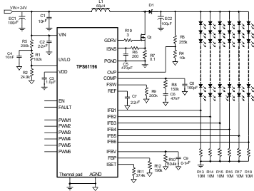
Simplified Schematic

4 Revision History
| DATE | REVISION | NOTES |
|---|---|---|
| March 2015 | * | Initial release. |