SLVSBO4C October 2012 – December 2014 TPS62736 , TPS62737
UNLESS OTHERWISE NOTED, this document contains PRODUCTION DATA.
- 1 Features
- 2 Applications
- 3 Description
- 4 Revision History
- 5 Description (continued)
- 6 Device Voltage Options
- 7 Pin Configuration and Functions
- 8 Specifications
- 9 Detailed Description
- 10Application and Implementation
- 11Power Supply Recommendations
- 12Layout
- 13Device and Documentation Support
- 14Mechanical, Packaging, and Orderable Information
Package Options
Mechanical Data (Package|Pins)
- RGY|14
Thermal pad, mechanical data (Package|Pins)
- RGY|14
Orderable Information
7 Pin Configuration and Functions
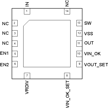
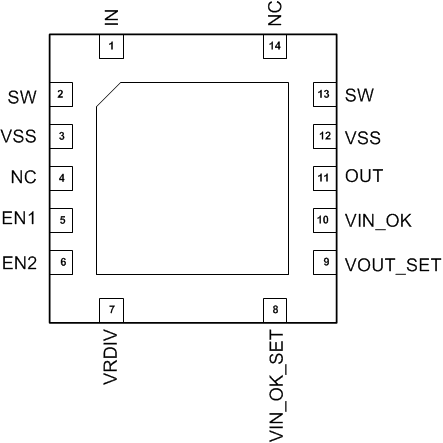
Pin Functions
| PIN | DESCRIPTION | |||
|---|---|---|---|---|
| NAME | TPS62736 RGY |
TPS62737 RGY |
TYPE | |
| EN1 | 5 | 5 | Input | Digital input for chip enable, standby, and ship-mode. EN1 = 1 sets ship mode independent of EN2. EN1=0, EN2 = 0 disables the buck converter and sets standby mode. EN1=0, EN2=1 enables the buck converter. Do not leave either pin floating. |
| EN2 | 6 | 6 | Input | |
| IN | 1 | 1 | Input | Input supply to the buck regulator |
| NC | 2, 3, 4, 14 | 4, 14 | Input | Connect to VSS |
| OUT | 11 | 11 | Output | Step down (buck) regulator output |
| SW | 13 | 2, 13 | Input | Inductor connection to switching node |
| Thermal Pad | 15 | 15 | Input | Connect to VSS |
| VIN_OK | 10 | 10 | Output | Push-pull digital output for power-good indicator for the input voltage. Pulled up to VIN pin. |
| VIN_OK_SET | 8 | 8 | Input | Resistor divider input for VIN_OK threshold. Pull to VIN to disable. Do not leave pin floating. |
| VOUT_SET | 9 | 9 | Input | Resistor divider input for VOUT regulation level |
| VRDIV | 7 | 7 | Output | Resistor divider biasing voltage |
| VSS | 12 | 3, 12 | Input | Ground connection for the device |