SLVSBJ1B September 2012 – January 2017 TPS65051-Q1
PRODUCTION DATA.
- 1 Features
- 2 Applications
- 3 Description
- 4 Revision History
- 5 Pin Configuration and Functions
- 6 Specifications
-
7 Detailed Description
- 7.1 Overview
- 7.2 Functional Block Diagram
- 7.3
Feature Description
- 7.3.1 Operation
- 7.3.2 DCDC1 Converter
- 7.3.3 DCDC2 Converter
- 7.3.4 Dynamic Voltage Positioning
- 7.3.5 Soft Start
- 7.3.6 100% Duty-Cycle Low-Dropout Operation
- 7.3.7 Undervoltage Lockout
- 7.3.8 Mode Selection
- 7.3.9 Enable
- 7.3.10 RESET
- 7.3.11 Short-Circuit Protection
- 7.3.12 Thermal Shutdown
- 7.3.13 Low Dropout Voltage Regulators
- 7.4 Device Functional Modes
- 8 Application and Implementation
- 9 Power Supply Recommendations
- 10Layout
- 11Device and Documentation Support
- 12Mechanical, Packaging, and Orderable Information
Package Options
Mechanical Data (Package|Pins)
- RSM|32
Thermal pad, mechanical data (Package|Pins)
- RSM|32
Orderable Information
1 Features
- Qualified for Automotive Applications
- AEC-Q100 Qualified With the Following Results:
- Device Temperature Grade 1: –40°C to +125°C Ambient Operating Temperature Range
- Device HBM ESD Classification Level H2
- Device CDM ESD Classification Level C3B
- Up To 95% Efficiency
- Output Current for DC-DC Converter:
DCDC1 = 1 A; DCDC2 = 0.6 A - Externally Adjustable Output Voltage for DC-DC Converter
- VI Range for DC-DC Converters
From 2.5 V to 6 V - 2.25-MHz Fixed-Frequency Operation
- Power-Save Mode at Light Load Current
- 180° Out-of-Phase Operation
- Output-Voltage Accuracy in PWM Mode ±1%
- Low-Ripple PFM Mode
- Total Typical 32-μA Quiescent Current for Both DC-DC Converters
- 100% Duty Cycle for Lowest Dropout
- Two General-Purpose 400-mA, High-PSRR LDOs
- Two General-Purpose 200-mA, High-PSRR LDOs
- VI Range for LDOs from 1.5 V to 6.5 V
- Digital Voltage Selection for the LDOs
- Available in a 4-mm × 4-mm 32-Pin VQFN Package
2 Applications
Automotive Infotainment
Automotive Cluster
Automotive Digital Radio
3 Description
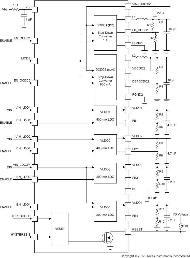
The TPS65051-Q1 device is an integrated power-management IC for applications powered by one Li-Ion or Li-Polymer cell, which requires multiple power rails. The TPS65051-Q1 device provides two efficient, 2.25-MHz step-down converters targeted at providing the core voltage and I/O voltage in a processor-based system. Both step-down converters enter a low-power mode at light load for maximum efficiency across the widest possible range of load currents.
For low-noise applications, the user can force the devices into fixed-frequency PWM mode by pulling the MODE pin high. Operating in the shutdown mode reduces the current consumption to less than 1 μA. The devices allow the use of small inductors and capacitors to achieve a small solution size. The TPS65051-Q1 device provides an output current of up to 1 A (DCDC1) and 0.6 A (DCDC2). The TPS65051-Q1 device also integrates two 400-mA LDO and two 200-mA LDO voltage regulators, which one can turn on or off using separate enable pins on each LDO. Each LDO operates with an input voltage range between 1.5 V and 6.5 V, allowing the supply to be from one of the step-down converters or directly from the main battery.
The LDO voltage of the TPS65051-Q1 device is adjustable using external resistor dividers.
Device Information(1)
| PART NUMBER | PACKAGE | BODY SIZE (NOM) |
|---|---|---|
| TPS65051-Q1 | VQFN (32) | 4.00 mm × 4.00 mm |
- For all available packages, see the orderable addendum at the end of the datasheet.
Block Diagram

4 Revision History
Changes from A Revision (November 2012) to B Revision
- Added Pin Configuration and Functions section, ESD Ratings table, Feature Description section, Device Functional Modes, Application and Implementation section, Power Supply Recommendations section, Layout section, Device and Documentation Support section, and Mechanical, Packaging, and Orderable Information sectionGo
- Deleted all references to TPS65050-Q1, TPS65052-Q1, TPS65054-Q1, and TPS65056-Q1 part numbers Go
- Deleted the Ordering Information tableGo
- Changed the resistor labels of R3, R4, and R5 to R13, R14, and R15 in the RESET sectionGo
- Added the Receiving Notification of Documentation Updates sectionGo
- Changed the electrostatic discharge statement Go