SLVSDJ1A July 2016 – May 2017 TPS65381A-Q1
PRODUCTION DATA.
- 1 Device Overview
- 2 Revision History
- 3 Pin Configuration and Functions
- 4 Specifications
-
5 Detailed Description
- 5.1 Overview
- 5.2 Functional Block Diagram
- 5.3 Feature Description
- 5.4
Device Functional Modes
- 5.4.1 Power-Up and Power-Down Behavior
- 5.4.2 Safety Functions and Diagnostics Overview
- 5.4.3 Voltage Monitor (VMON)
- 5.4.4 TPS65381A-Q1 Internal Error Signals
- 5.4.5 Loss-of-Clock Monitor (LCMON)
- 5.4.6 Analog Built-In Self-Test (ABIST)
- 5.4.7 Logic Built-In Self-Test (LBIST)
- 5.4.8 Junction Temperature Monitoring and Current Limiting
- 5.4.9 Diagnostic MUX and Diagnostic Output Pin (DIAG_OUT)
- 5.4.10 Watchdog Timer (WD)
- 5.4.11 Watchdog Fail Counter, Status, and Fail Event
- 5.4.12 Watchdog Sequence
- 5.4.13 MCU to Watchdog Synchronization
- 5.4.14 Trigger Mode (Default Mode)
- 5.4.15 Q&A Mode
- 5.4.16 MCU Error Signal Monitor (MCU ESM)
- 5.4.17 Device Configuration Register Protection
- 5.4.18 Enable and Reset Driver Circuit
- 5.4.19 Device Operating States
- 5.4.20 STANDBY State
- 5.4.21 RESET State
- 5.4.22 DIAGNOSTIC State
- 5.4.23 ACTIVE State
- 5.4.24 SAFE State
- 5.4.25 State Transition Priorities
- 5.4.26 Power on Reset (NPOR)
- 5.5
Register Maps
- 5.5.1 Serial Peripheral Interface (SPI)
- 5.5.2 SPI Register Write Access Lock (SW_LOCK command)
- 5.5.3 SPI Registers (SPI Mapped Response)
- 5.5.4
Device Safety Status and Control Registers
- 5.5.4.1 VMON_STAT_1 Register
- 5.5.4.2 VMON_STAT_2 Register
- 5.5.4.3 SAFETY_STAT_1 Register
- 5.5.4.4 SAFETY_STAT_2 Register
- 5.5.4.5 SAFETY_STAT_3 Register
- 5.5.4.6 SAFETY_STAT_4 Register
- 5.5.4.7 SAFETY_STAT_5 Register
- 5.5.4.8 SAFETY_ERR_CFG Register
- 5.5.4.9 SAFETY_BIST_CTRL Register
- 5.5.4.10 SAFETY_CHECK_CTRL Register
- 5.5.4.11 SAFETY_FUNC_CFG Register
- 5.5.4.12 SAFETY_ERR_STAT Register
- 5.5.4.13 SAFETY_ERR_PWM_H Register
- 5.5.4.14 SAFETY_ERR_PWM_L Register
- 5.5.4.15 SAFETY_PWD_THR_CFG Register
- 5.5.4.16 SAFETY_CFG_CRC Register
- 5.5.4.17 Diagnostics
- 5.5.5 Watchdog Timer
- 5.5.6 Sensor Supply
-
6 Application and Implementation
- 6.1 Application Information
- 6.2
Typical Application
- 6.2.1 Design Requirements
- 6.2.2
Detailed Design Procedure
- 6.2.2.1 VDD6 Preregulator
- 6.2.2.2 VDD1 Linear Controller
- 6.2.2.3 VSOUT1 Tracking Linear Regulator, Configured to Track VDD5
- 6.2.2.4 Alternative Use for VSOUT1 Tracking Linear Regulator, Configured for 6-V Output Tracking VDD3/5 In 3.3-V Mode
- 6.2.2.5 Alternative Use for VSOUT1 Tracking Linear Regulator, Configured for 9-V Output Tracking to 5-V Input from VDD5
- 6.2.2.6 Alternative Use for VSOUT1 Tracking Linear Regulator, Configured in Non-tracking Mode Providing a 4.5-V Output
- 6.2.3 Application Curves
- 6.3 System Examples
- 7 Power Supply Recommendations
- 8 Layout
- 9 Device and Documentation Support
- 10Mechanical, Packaging, and Orderable Information
Package Options
Mechanical Data (Package|Pins)
- DAP|32
Thermal pad, mechanical data (Package|Pins)
- DAP|32
Orderable Information
8 Layout
8.1 Layout Guidelines
8.1.1 VDD6 Buck Preregulator
- Minimize the loop area for the switching loop of the inductor, ESR resistor, output capacitor, and diode.
- Minimize the parasitic trace impedance by using traces that are as wide as possible.
- Minimize the parasitic via impedance by using multiple vias, especially on high current and switching nodes.
- Connect the inductor and diode to SDN6 as close as possible to the pin.
- Connect the diode to PGND (ground plane).
- Connect the ESR resistor and output capacitor in series between VDD6 output (inductor output) and PGND.
- Connect the EMC filter capacitor between VDD6 output and PGND.
- Connect the VDD6 output to the VDD6 pin with routing to avoid coupling switching noise. Trace length should be minimized and as wide a trace as possible. This trace is the supply input to the downstream regulators using VDD6 as a preregulator, parasitic impedance should be minimized.
Additional consideration: add a footprint for a RC snubber circuit if one is required for the application. The RC connects in-series between the SDN6 and PGND pins.
8.1.2 VDD1 Linear Regulator Controller
- Connect the drain of the external FET to VDD6 node, the trace should be minimized so that additional downstream buffering capacitors are not needed.
- Connect the output capacitor to the source of the external FET, the length of this trace should be minimized. Connect the output capacitor to the ground plane.
- Connect the gate drive, VDD1_G, to the gate of the FET. Connect the resistor between the gate of the FET and the source of the FET, minimize the trace length.
- The resistor divider for sensing and setting the output voltage connects between the source of the FET (VDD1 output) and GND (device signal ground). Do not locate these components and their traces near the switching nodes or high-current traces.
8.1.3 VDD5 and VDD3/5 Linear Regulators
Connect the output capacitor as close as possible between the VDDx output and GND.
8.1.4 VSOUT1 Tracking Linear Regulator
- Connect the output capacitor as close as possible between the VSOUT1 output and GND.
- The resistor divider for sensing and setting the output voltage connects between the VSOUT1 and GND (device signal ground). Do not locate these components and their traces near the switching nodes or high-current traces.
- Connect the local decoupling capacitor between the VSIN and PGND pins. Minimize trace length.
- Route the tracking supply signal, connected to VTRACK1, away from switching nodes or high-current traces.
8.1.5 Charge Pump
- Connect the capacitor as close as possible between the CP1 and CP2 pins.
- Connect the capacitor between the VCP pin and VBATP (reverse protected and filtered) supply.
8.1.6 Other Considerations
- Use ground planes. TI recommends having a solid ground plane and connect GND and PGND with as low impendence paths as possible to the ground plane.
- Minimize parasitic impedance on the critical switching and high current paths.
- Short PGNDx and GND to the thermal pad.
- Use a star ground configuration if connecting to a non-ground plane system. Use tie-ins for the voltage-sense feedback ground and local biasing bypass capacitor ground networks to this star ground.
- Connect the local decoupling capacitor between VBATP and PGND. Minimize trace length.
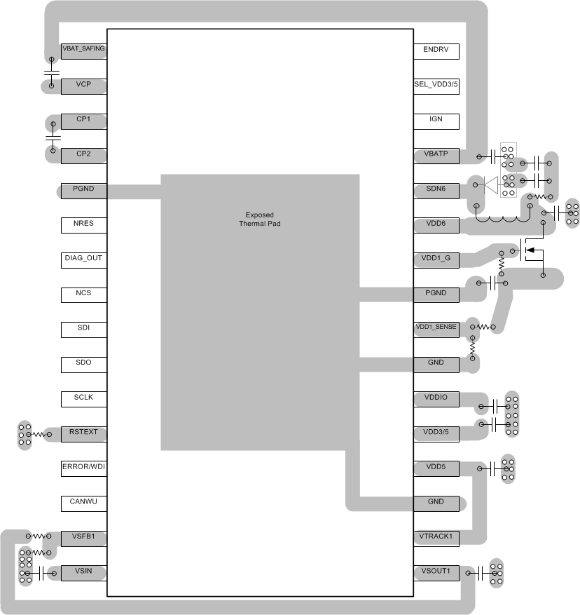
8.2 Layout Example
 Figure 8-1 TPS65381A-Q1 Board Layout
8.3 Power Dissipation and Thermal Considerations
The power dissipation of the device in the application has significant impact on the necessary layout and thermal management strategy of the application.
Use the following equations to calculate the estimated power dissipation in the device:
where
- PVDD6 is a conservative estimation of the power dissipation of VDD6 in the device because some of the efficiency loss is externally in the diode and inductor. A more accurate power estimator is available in the TPS65381-Q1 and TPS65381A-Q1 Power Estimator.
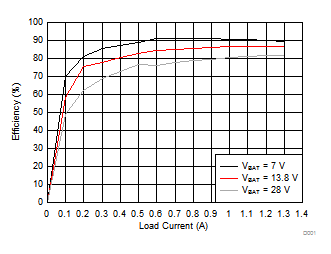
- effVDD6 is the efficiency of VDD6 buck preregulator according to Figure 8-2 .
- IVDD6 is the total load current from VDD5, VDD3/5, VDD1, VSOUT1 and any external load connected to VDD6.
where
- IVDD5 is the load current on VDD5.
where
- VVDD3/5 is either 3.3 V or 5 V.
- IVDD3/5 is the load current on VDD3/5.
where
- VVSIN is either 6 V (VDD6) or VBATP.
- VVSOUT1 is the programmed output voltage of VSOUT1.
- IVSOUT1 is the load current on VSOUT1
where
- PTOT is the total power dissipation in the device.
 Figure 8-2 Typical VDD6 BUCK Efficiency
The useful range of device operation is affected by the supply voltage, application load-current requirements, and the thermal characteristics of the package and printed circuit board (PCB). For the device to be useful over a wide temperature range, the package, PCB and thermal management strategy must allow for the effective removal of the produce heat to keep junction temperature of the device within rated limits.
Use Equation 1 to Equation 5 to calculate the estimated power dissipation. As shown by the equation for VDD6 power dissipation (PVDD6), Equation 2, a large portion of the power dissipation is determined by the efficiency of the VDD6 supply. The efficiency of the VDD6 supply depends on load current and supply voltage as shown in Equation 2.
The 32-pin HTSSOP PowerPAD (DAP) offers an effective means of removing heat from the device junction. As described in PowerPad™ Thermally Enhanced Package, the PowerPAD package offers a lead-frame die pad that is exposed at the base of the package. This thermal pad must be soldered to the copper on the PCB directly underneath the package to create an effective path for removal of heat from the device, and, therefore, to reduce the RθJC. The PCB must be designed with thermal lands and thermal vias to complete the heat removal subsystem, as summarized in PowerPAD™ Made Easy and A Guide to Board Layout for Best Thermal Resistance for Exposed Packages.
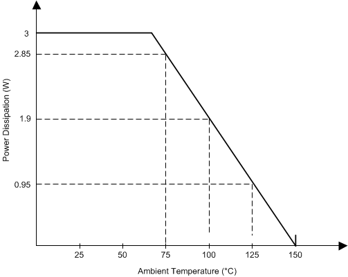
Figure 8-3 shows the thermal derating profile of the 32-pin HTSSOP (DCA) Package With PowerPAD according to RθJA as specified in Section 4.4.

Considering the power dissipation of the device in the specific application is important, which is highly dependent on the supply voltage and load currents, the ambient and board temperatures, and any additional heat sink or cooling strategies necessary to maintain the junction temperature of the device below the maximum junction temperature of 150°C.
NOTE
The VDD1 regulator may have significant power dissipation in the external FET depending on the VDD1 voltage and load current. The external FET power dissipation for the VDD1 regulator must be considered in system-level thermal analysis. If better efficiency or thermal performance is needed, a DC-DC regulator could be used instead of the linear regulator controller with external FET. The output voltage of the DC-DC regulator can still be monitored by the VDD1_SENSE pin similar to the VDD1 output voltage when the VDD1 linear regulator controller is used with an external FET.
NOTE
The PowerPAD thermal pad is not directly connected to any leads of the package. However, it is electrically and thermally connected to the substrate, which is the ground (GND) and power ground (PGND) of the device.
NOTE
Additional information about thermal analysis and design can be found on www.ti.com in the WEBENCH® Design Center thermal analysis section.