SWCS046U March 2010 – October 2014 TPS65910
PRODUCTION DATA.
- 1Device Overview
- 2Revision History
- 3 Device Comparison
- 4Terminal Configuration and Functions
-
5Specifications
- 5.1 Absolute Maximum Ratings
- 5.2 Handling Ratings
- 5.3 Recommended Operating Conditions
- 5.4 Thermal Resistance Characteristics for RSL Package
- 5.5 I/O Pullup and Pulldown Characteristics
- 5.6 Digital I/O Voltage Electrical Characteristics
- 5.7 I2C Interface and Control Signals
- 5.8 Power Consumption
- 5.9 Power References and Thresholds
- 5.10 Thermal Monitoring and Shutdown
- 5.11 32-kHz RTC Clock
- 5.12 Backup Battery Charger
- 5.13 VRTC LDO
- 5.14 VIO SMPS
- 5.15 VDD1 SMPS
- 5.16 VDD2 SMPS
- 5.17 VDD3 SMPS
- 5.18 VDIG1 and VDIG2 LDO
- 5.19 VAUX33 and VMMC LDO
- 5.20 VAUX1 and VAUX2 LDO
- 5.21 VDAC and VPLL LDO
- 5.22
Timing and Switching Characteristics
- 5.22.1 Switch-On/-Off Sequences and Timing
- 5.22.2
Power Control Timing
- 5.22.2.1 Device Turn-On/Off With Rising/Falling Input Voltage
- 5.22.2.2 Device State Control Through PWRON Signal
- 5.22.2.3 Device SLEEP State Control
- 5.22.2.4 Power Supplies State Control Through the SCLSR_EN1 and SDASR_EN2 Signals
- 5.22.2.5 VDD1 and VDD2 Voltage Control Through SCLSR_EN1 and SDASR_EN2 Signals
- 5.22.2.6 SMPS Switching Synchronization
-
6Detailed Description
- 6.1 Power Reference
- 6.2 Power Sources
- 6.3 Embedded Power Controller
- 6.4 32-kHz RTC Clock
- 6.5 RTC
- 6.6 Backup Battery Management
- 6.7 Backup Registers
- 6.8 I2C Interface
- 6.9 Thermal Monitoring and Shutdown
- 6.10 Interrupts
- 6.11 Package Description
- 6.12 Functional Registers
- 7Device and Documentation Support
- 8Mechanical Packaging and Orderable Information
Package Options
Mechanical Data (Package|Pins)
- RSL|48
Thermal pad, mechanical data (Package|Pins)
- RSL|48
Orderable Information
6 Detailed Description
6.1 Power Reference
The bandgap voltage reference is filtered by using an external capacitor connected across the VREF output and the analog ground REFGND (see Section 5.3, Recommended Operating Conditions). The VREF voltage is distributed and buffered inside the device.
6.2 Power Sources
The power resources provided by the TPS65910 device include inductor-based switched mode power supplies (SMPS) and linear low drop-out voltage regulators (LDOs). These supply resources provide the required power to the external processor cores and external components, and to modules embedded in the TPS65910 device.
Two of these SMPS have DVS capability SmartReflex Class 3 compatible. These SMPS provide independent core voltage domains to the host processor. The remaining SMPS provides supply voltage for the host processor I/Os.
Table 6-1 lists the power sources provided by the TPS65910 device.
Table 6-1 Power Sources
| RESOURCE | TYPE | VOLTAGES | POWER |
|---|---|---|---|
| VIO | SMPS | 1.5 V / 1.8 V / 2.5 V / 3.3 V | 1000 mA |
| VDD1 | SMPS | 0.6 ... 1.5 in 12.5-mV steps | 1500 mA |
| Programmable multiplication factor: x2, x3 | |||
| VDD2 | SMPS | 0.6 ... 1.5 in 12.5-mV steps | 1500 mA |
| Programmable multiplication factor: x2, x3 | |||
| VDD3 | SMPS | 5 V | 100 mA |
| VDIG1 | LDO | 1.2 V, 1.5 V, 1.8 V, 2.7 V | 300 mA |
| VDIG2 | LDO | 1 V, 1.1 V, 1.2 V, 1.8 V | 300 mA |
| VPLL | LDO | 1.0 V, 1.1 V, 1.8 V, 2.5 V | 50 mA |
| VDAC | LDO | 1.8 V, 2.6 V, 2.8 V, 2.85 V | 150 mA |
| VAUX1 | LDO | 1.8 V, 2.5 V, 2.8 V, 2.85 V | 300 mA |
| VAUX2 | LDO | 1.8 V, 2.8 V, 2.9 V, 3.3 V | 150 mA |
| VAUX33 | LDO | 1.8 V, 2.0 V, 2.8 V, 3.3 V | 150 mA |
| VMMC | LDO | 1.8 V, 2.8 V, 3.0 V, 3.3 V | 300 mA |
6.3 Embedded Power Controller
The embedded power controller manages the state of the device and controls the power-up sequence.
6.3.1 State-Machine
The EPC supports the following states:
No supply: The main battery supply voltage is not high enough to power the VRTC regulator. A global reset is asserted in this case. Everything on the device is off.
Backup: The main battery supply voltage is high enough to enable the VRTC domain but not enough to switch on all the resources. In this state, the VRTC regulator is in backup mode and only the 32-K oscillator and RTC module are operating (if enabled). All other resources are off or under reset.
Off: The main battery supply voltage is high enough to start the power-up sequence but device power on is not enabled. All power supplies are in OFF state except VRTC.
Active: Device power-on enable conditions are met and regulated power supplies are on or can be enabled with full current capability.
Sleep: Device SLEEP enable conditions are met and some selected regulated power supplies are in low-power mode.
Figure 6-1 shows the transitions of the state-machine.
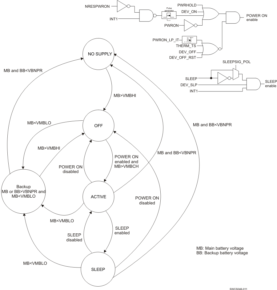 Figure 6-1 Embedded Power Control State-Machine
Device power-on enable conditions:
If none of the device power-on disable conditions is met, the following conditions are available to turn on and/or maintain the ON state of the device:
- PWRON signal low level.
- Or PWRHOLD signal high level.
- Or DEV_ON control bit set to 1 (default inactive).
- Or interrupt flag active (default INT1 low) while the device is off (NRESPWRON = 0) generates a power-on enable condition during a fixed delay (TDOINT1 pulse duration defined in Section 5.22.2, Power Control Timing).
The power-on enable condition pulse occurs only if the interrupt status bit is initially low (no previous identical interrupt pending in the status register).
The Interrupt sources expected when the device is off are:
- PWRON low-level interrupt (PWRON_IT = 1 in INT_STS_REG register)
- PWRHOLD rising-edge interrupt (PWRHOLD_IT = 1 in INT_STS_REG register)
The Interrupt sources expected if enabled when the device is off are:
- RTC Alarm interrupt (RTC_ALARM_IT = 1 or RTC_PERIOD_IT = 1 in INT_STS_REG register)
- First-time input voltage rising above VMBHI threshold (Boot mode or EEPROM dependent) and input voltage > VMBCH threshold (VMBCH_IT = 1 in INT_STS_REG register).
GPIO_CKSYNC cannot be used to turn on the device (OFF-to-ACTIVE state transition), even if its associated interrupt is not masked, but can be used as an interrupt source to wake up the device from SLEEP-to-ACTIVE state.
Device power-on disable conditions:
- PWRON signal low level during more than the long-press delay: tdPWRONLP (can be disabled though register programming). The interrupt corresponding to this condition is PWRON_LP_IT in the INT_STS_REG register.
- Or Die temperature has reached the thermal shutdown threshold.
- Or DEV_OFF or DEV_OFF_RST control bit set to 1 (value of DEV_OFF is cleared when the device is in OFF state).
Device SLEEP enable conditions:
- SLEEP signal low level (default, or high level depending on the programmed polarity)
- And DEV_SLP control bit set to 1
- And interrupt flag inactive (default INT1 high): no nonmasked interrupt pending
The SLEEP state can be controlled by programming DEV_SLP and keeping the SLEEP signal in the active polarity state, or it can be controlled through the SLEEP signal setting the DEV_SLP bit to 1 once, after device turn-on.
6.3.2 Switch-On/-Off Sequences
The power sequence is the automated switching on of the device resources when an off-to-active transition takes place.
The device supports three embedded power sequences selectable by the device BOOT pins.
| BOOT0 | BOOT1 | Processor Supported |
|---|---|---|
| 0 | 0 | AM3517, AM3505 |
| 1 | 0 | OMAP3 Family, AM3715/03, DM3730/25 |
| 0 | 1 | EEPROM sequence |
Details of the boot sequence timing are given in Section 5.22.1. EEPROM sequences can be used for specific power up sequence for corresponding application processor. For details of EEPROM sequence refer to the user guides on the product folder: http://focus.ti.com/docs/prod/folders/print/tps65910.html.
6.3.3 Control Signals
6.3.3.1 SLEEP
When none of the device sleep-disable conditions are met, a falling edge (default, or rising edge, depending on the programmed polarity) of this signal causes an ACTIVE-to-SLEEP state transition of the device. A rising edge (default, or falling edge, depending on the programmed polarity) causes a transition back to ACTIVE state. This input signal is level sensitive and no debouncing is applied.
While the device is in SLEEP state, predefined resources are automatically set in their low-power mode or off. Resources can be kept in their active mode: (full-load capability), programming the SLEEP_KEEP_LDO_ON and the SLEEP_KEEP_RES_ON registers. These registers contain 1 bit per power resource. If the bit is set to 1, then that resource stays in active mode when the device is in SLEEP state. 32KCLKOUT is also included in the SLEEP_KEEP_RES_ON register and the 32-kHz clock output is maintained in SLEEP state if the corresponding mask bit is set.
6.3.3.2 PWRHOLD
When none of the device power-on disable conditions are met, a rising edge of this signal causes an OFF-to-ACTIVE state transition of the device and a falling edge causes a transition back to OFF state. Typically, this signal is used to control the device in a slave configuration. It can be connected to the SYSEN output signal from other TPS659xx devices, or the NRESPWRON signal of another TPS65910 device. This input signal is level sensitive and no debouncing is applied.
A rising edge of PWRHOLD is highlighted though an associated interrupt.
6.3.3.3 BOOT0/BOOT1
These signals determine which processor the device is working with and hence which power-up sequence is needed. See Section 5.22.1 for more details. There is no debouncing on this input signal.
6.3.3.4 NRESPWRON
This signal is used as the reset to the processor. It is held low until the ACTIVE state is reached. See Section 5.22.2 to get detailed timing.
6.3.3.5 CLK32KOUT
This signal is the output of the 32K oscillator, which can be enabled or not during the power-on sequence, depending on the Boot mode. It can be enabled and disabled by register bit, during ACTIVE state of the device. CLK32KOUT output can also be enabled or not during SLEEP state of the device depending on the SLEEPMASK register programming.
6.3.3.6 PWRON
A falling edge on this signal causes after tdbPWRONF debouncing delay (defined in Figure 5-4 and Table 5-5) an OFF-to-ACTIVE state or SLEEP-to-ACTIVE state transition of the device and makes the corresponding interrupt (PWRON_IT) active. The PWRON input is connected to an external push-button. The built-in debouncing time defines a minimum button press duration that is required for button press detection. Any button press duration which is lower than this value is ignored, considered an accidental touch.
After an OFF-to-ACTIVE state transition, the PMIC maintains ACTIVE during tdOINT delay, if the button is released. After this delay if none of the device enabling conditions is set by the processor supplied, the PMIC automatically turns off. If the button is not released, the PMIC maintains ACTIVE up to tdPWRONLPTO, because PWRON low is a device enabling condition. After a SLEEP-to-ACTIVE state transition, the PMIC maintains ACTIVE as long as an interrupt is pending.
If the device is already in ACTIVE state, a PWRON low level makes the corresponding interrupt (PWRON_IT) active.
When the PMIC is in ACTIVE mode, if the button is pressed for longer time than tdPWRONLP, the PMIC generates the PWON_LP_IT interrupt. If the processor does not acknowledge the long press interrupt within a period of tdPWRONLPTO – tdPWRONLP, the PMIC goes to OFF mode and shuts down the DCDCs and LDOs.
6.3.3.7 INT1
INT1 signal (default active low) warns the host processor of any event that occurred on the TPS65910 device. The host processor can then poll the interrupt from the interrupt status register through I2C to identify the interrupt source. A low level (default setting) indicates an active interrupt, highlighted in the INT_STS_REG register. The polarity of INT1 can be set by programming the IT_POL control bit.
Any (not masked or masked) interrupt detection causes a POWER ON enable condition during a fixed delay tDOINT1 (only) when the device is in OFF state (when NRESPWON signal is low). Any (not masked) interrupt detection is causing a device wakeup from SLEEP state up to acknowledge of the pending interrupt. Any of the interrupt sources can be masked by programming the INT_MSK_REG register. When an interrupt is masked, its corresponding interrupt status bit is still updated, but the INT1 flag is not activated.
Interrupt source masking can be used to mask a device switch-on event. Because interrupt flag active is a POWER ON enable condition during tDOINT1 delay, any interrupt not masked must be cleared to allow turn off of the device after the tDOINT1 POWER ON enable pulse duration.. See section: Interrupts, for interrupt sources definition.
6.3.3.8 SDASR_EN2 and SCLSR_EN1
SDASR_EN2 and SCLSR_EN1 are the data and clock signals of the serial control interface (SR-I2C) dedicated to SmartReflex applications. These signals can also be programmed to be used as enable signals of one or several supplies, when the device is on (NRESPWRON high). A resource assigned to SDASR_EN2 or SCLSR_EN1 control automatically disables the serial control interface.
Programming EN1_LDO_ASS_REG, EN2_LDO_REG, and SLEEP_KEEP_LDO_ON_REG registers: SCLSR_EN1 and SDASR_EN2 signals can be used to control the turn on/off or sleep state of any LDO type supplies.
Programming EN1_SMPS_ASS_REG, EN2_SMPS_ASS_REG, and SLEEP_KEEP_RES_ON registers: SCLSR_EN1 and SDASR_EN2 signals can be used to control the turn on/off or low-power state (PFM mode) of SMPS type supplies.
SDASR_EN2 and SCLSR_EN1 can be used to set output voltage of VDD1 and VDD2 SMPS from a roof to a floor value, preprogrammed in the VDD1_OP_REG, VDD2_OP_REG, and teh VDD1_SR_REG, VDD2_SR_REG registers. Tun-off of VDD1 and VDD2 can also be programmed either in VDD1_OP_REG, VDD2_OP_REG or in VDD1_SR_REG, VDD2_SR_REG registers.
When a supply is controlled through SCLSR_EN1 or SCLSR_EN2 signals, its state is no longer driven by the device SLEEP state.
6.3.3.9 GPIO_CKSYNC
GPIO_CKSYNC is a configurable open-drain digital I/O: directivity, debouncing delay and internal pullup can be programmed in the GPIO0_REG register. GPIO_CKSYNC cannot be used to turn on the device (OFF-to-ACTIVE state transition), even if its associated interrupt is not masked, but can be used as an interrupt source to wake up the device from SLEEP-to-ACTIVE state.
Programming DCDCCKEXT = 1, VDD1, VDD2, VIO, and VDD3 DC-DC switching can be synchronized using a 3-MHz clock set though the GPIO_CKSYNC pin.
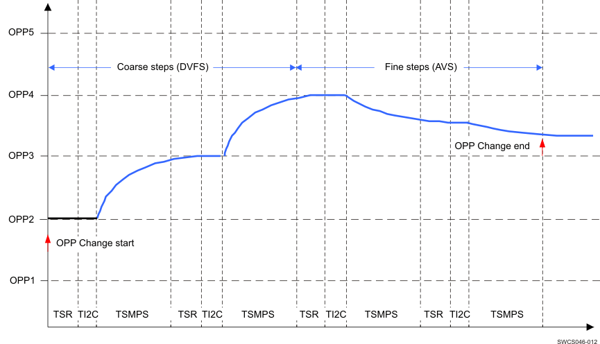
6.3.4 Dynamic Voltage Frequency Scaling and Adaptive Voltage Scaling Operation
Dynamic voltage frequency scaling (DVFS) operation: a supply voltage value corresponding to a targeted frequency of the digital core supplied is programmed in VDD1_OP_REG or VDD2_OP_REG registers.
The slew rate of the voltage supply reaching a new VDD1_OP_REG or VDD2_OP_REG programmed value is limited to 12.5 mV/µs, fixed value. Adaptative voltage scaling (AVS) operation: a supply voltage value corresponding to a supply voltage adjustment is programmed in VDD1_SR_REG or VDD2_SR_REG registers. The supply voltage is then intended to be tuned by the digital core supplied, based its performance self-evaluation. The slew rate of VDD1 or VDD2 voltage supply reaching a new programmed value is programmable though the VDD1_REG or VDD2_REG register, respectively.
A serial control interface (SR-I2C) is dedicated to SmartReflex applications such as DVFS and class 3 AVS, and thus gives access to the VDD1_OP_REG, VDD1_SR_REG, and VDD2_OP_REG, VDD2_SR_REG register.
A general-purpose serial control interface (CTL-I2C) also gives access to these registers, if SR_CTL_I2C_SEL control bit is set to 1 in the DEVCTRL_REG register (default inactive).
Both control interfaces are compliant with HS-I2C specification (100 kbps, 400 kbps, or 3.4 Mbps).
Figure 6-2 shows an example of a SmartReflex operation. To optimize power efficiency, the voltage domains of the host processor uses the DVFS and AVS features provided by SmartReflex.
6.4 32-kHz RTC Clock
The TPS65910 device can provide a 32-kHz clock to the platform through the CLK32KOUT output, the source of this 32-kHz clock can be:
- 32-kHz crystal connected from OSC32IN to OSC32KOUT pins
- A square-wave 32-kHz clock signal applied to OSC32IN input (OSC32KOUT kept floating).
- Internal 32-kHz RC oscillator, to reduce the BOM, if an accurate clock is not needed by the system.
Default selection of a 32-kHz RC oscillator versus 32-kHz crystal oscillator or external square-wave 32-kHz clock depends on the Boot mode or device version (EEPROM programming):
- BOOT1 = 0, BOOT0 = 1: quartz oscillator or external square wave 32-kHz clock default
- BOOT1 = 0, BOOT0 = 0: 32-kHz RC oscillator default
Switching from the 32-kHz RC oscillator to the 32-kHz crystal oscillator or external square-wave 32-kHz clock can also be programmed though DEVCTRL_REG register, taking benefit of the shorter turn-on time of the internal RC oscillator.
Switching from the 32-kHz crystal oscillator or external square-wave clock to the RC oscillator is not supported.
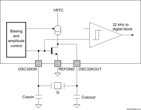 Figure 6-3 Crystal Oscillator 32-kHz Clock
6.5 RTC
The RTC, which is driven by the 32-kHz clock, provides the alarm and timekeeping functions. The RTC is kept supplied when the device is in the OFF or the BACKUP state.
The main functions of the RTC block are:
- Time information (seconds/minutes/hours) directly in binary-coded decimal (BCD) format
- Calendar information (Day/Month/Year/Day of the week) directly in BCD code up to year 2099
- Programmable interrupts generation: The RTC can generate two interrupts: a timer interrupt RTC_PERIOD_IT periodically (1s/1m/1h/1d period) and an alarm interrupt RTC_ALARM_IT at a precise time of the day (alarm function). These interrupts are enabled using IT_ALARM and IT_TIMER control bits. Periodically interrupts can be masked during the SLEEP period to avoid host interruption and are automatically unmasked after SLEEP wakeup (using the IT_SLEEP_MASK_EN control bit).
- Oscillator frequency calibration and time correction
 Figure 6-4 RTC Digital Section Block Diagram
NOTE
INT_ALARM can generate a wakeup of the platform.
INT_TIMER cannot generate a wakeup of the platform.
6.5.1 Time Calendar Registers
All the time and calendar information are available in these dedicated registers, called TC registers. Values of the TC registers are written in BCD format.
- Year data ranges from 00 to 99
- Leap year = Year divisible by four (2000, 2004, 2008, 2012...)
- Common year = other years
- Month data ranges from 01 to 12
- Day value ranges from:
- 1 to 31 when months are 1, 3, 5, 7, 8, 10, 12
- 1 to 30 when months are 4, 6, 9, 11
- 1 to 29 when month is 2 and year is a leap year
- 1 to 28 when month is 2 and year is a common year
- Week value ranges from 0 to 6
- Hour value ranges from 00 to 23 in 24-hour mode and ranges from 1 to 12 in AM/PM mode
- Minutes value ranges from 0 to 59
- Seconds value ranges from 0 to 59
To modify the current time, software writes the new time into TC registers to fix the time/calendar information. The DBB can write into TC registers without stopping the RTC. In addition, software can stop the RTC by clearing the STOP_RTC bit of the control register and check the RUN bit of the status to be sure that the RTC is frozen. Then update TC values, and then restart the RTC by setting the STOP_RTC bit.
Example: Time is 10H54M36S PM (PM_AM mode set), 2008 September 5, previous register values are:
| Register | Value |
|---|---|
| SECONDS_REG | 0x36 |
| MINUTES_REG | 0x54 |
| HOURS_REG | 0x90 |
| DAYS_REG | 0x05 |
| MONTHS_REG | 0x09 |
| YEARS_REG | 0x08 |
The user can round to the closest minute, by setting the ROUND_30S register bit. TC values are set to the closest minute value at the next second. The ROUND_30S bit is automatically cleared when the rounding time is performed.
Example:
- If current time is 10H59M45S, a round operation changes time to 11H00M00S.
- if current time is 10H59M29S, a round operation changes time to 10H59M00S.
6.5.2 General Registers
Software can access the RTC_STATUS_REG and RTC_CTRL_REG registers at any time (except for the RTC_CTRL_REG[5] bit, which must be changed only when the RTC is stopped).
6.5.3 Compensation Registers
The RTC_COMP_MSB_REG and RTC_COMP_LSB_REG registers must respect the available access period. These registers must be updated before each compensation process. For example, software can load the compensation value into these registers after each hour event, during an available access period.
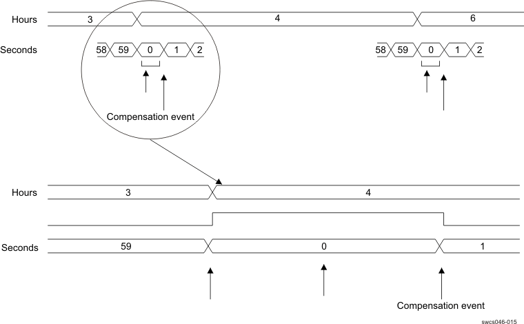 Figure 6-5 RTC Compensation Scheduling
This drift can be balanced to compensate for any inaccuracy of the 32-kHz oscillator. Software must calibrate the oscillator frequency, calculate the drift compensation versus one time hour period; and then load the compensation registers with the drift compensation value. Indeed, if the AUTO_COMP_EN bit in the RTC_CTRL_REG is enabled, the value of COMP_REG (in twos-complement) is added to the RTC 32-kHz counter at each hour and one second. When COMP_REG is added to the RTC 32-kHz counter, the duration of the current second becomes (32768 - COMP_REG)/32768s; so, the RTC can be compensated with a 1/32768 s/hour time unit accuracy.
NOTE
The compensation is considered once written into the registers.
6.6 Backup Battery Management
The device includes a back-up battery switch connecting the VRTC regulator input to a main battery (VCC7) or to a back-up battery (VBACKUP), depending on the batteries voltage value.
The VRTC supply can then be maintained during a BACKUP state as far as the input voltage is high enough (>VBNPR threshold). Below the VBNPR voltage threshold the digital core of the device is set under reset by internal signal POR (Power-on Reset).
The back-up domain functions which are always supplied from VRTC comprehend:
- The internal 32-kHz oscillator
- Backup registers
The back-up battery can be charged from the main battery through an embedded charger. The back-up battery charge voltage and enable is controlled through BBCH_REG register programming. This register content is maintained during the device Backup state.
Hence enabled the back-up battery charge is maintained as far as the main battery voltage is higher than the VMBLO threshold and the back-up battery voltage.
6.7 Backup Registers
As part of the RTC the device contains five 8-bit registers which can be used for storage by the application firmware when the external host is powered down. These registers retain their content as long as the VRTC is active.
6.8 I2C Interface
A general-purpose serial control interface (CTL-I2C) allows read and write access to the configuration registers of all resources of the system.
A second serial control interface (SR-I2C) is dedicated to SmartReflex applications such as DVFS or AVS.
Both control interfaces are compliant with HS-I2C specification.
These interfaces support the standard slave mode (100 Kbps), Fast mode (400 Kbps), and high-speed mode (3.4 Mbps). The general-purpose I2C module using one slave hard-coded address (ID1 = 2Dh). The SmartReflex I2C module uses one slave hard-coded address (ID0 = 12h). The master mode is not supported.
Addressing: Seven-bit mode addressing device
They do not support the following features:
- 10-bit addressing
- General call
6.9 Thermal Monitoring and Shutdown
A thermal protection module monitors the junction temperature of the device versus two thresholds:
- Hot-die temperature threshold
- Thermal shutdown temperature threshold
When the hot-die temperature threshold is reached an interrupt is sent to software to close the noncritical running tasks.
When the thermal shutdown temperature threshold is reached, the TPS65910 device is set under reset and a transition to OFF state is initiated. Then the power-on enable conditions of the device is not considered until the die temperature has decreased below the hot-die threshold. An hysteresis is applied to the hot-die and shutdown threshold, when detecting a falling edge of temperature, and both detection are debounced to avoid any parasitic detection. The TPS65910 device allows programming of four hot-die temperature thresholds to increase the flexibility of the system.
By default, the thermal protection is enabled in ACTIVE state, but can be disabled through programming register THERM_REG. The thermal protection can be enabled in SLEEP state programming register SLEEP_KEEP_RES_ON. The thermal protection is automatically enabled during an OFF-to-ACTIVE state transition and is kept enabled in OFF state after a switch-off sequence caused by a thermal shutdown event. Transition to OFF state sequence caused by a thermal shutdown event is highlighted in the INT_STS_REG status register. Recovery from this OFF state is initiated (switch-on sequence) when the die temperature falls below the hot-die temperature threshold.
Hot-die and thermal shutdown temperature threshold detections state can be monitored or masked by reading or programming the THERM_REG register. Hot-die interrupt can be masked by programming the INT_MSK_REG register.
6.10 Interrupts
Table 6-2 Interrupt Sources
| Interrupt | Description |
|---|---|
| RTC_ALARM_IT | RTC alarm event: Occurs at programmed determinate date and time |
| (running in ACTIVE, OFF, and SLEEP state, default inactive) | |
| RTC_PERIOD_IT | RTC periodic event: Occurs at programmed regular period of time (every second or minute) (running in ACTIVE, OFF, and SLEEP state, default inactive) |
| HOT_DIE_IT | The embedded thermal monitoring module has detected a die temperature above the hot-die detection threshold (running in ACTIVE and SLEEP state) |
| Level sensitive interrupt. | |
| PWRHOLD_IT | PWRHOLD signal rising edge |
| PWRON_LP_IT | PWRON is low during more than the long-press delay: tdPWRONLP (can be disable though register programming). |
| PWRON_IT | PWRON is low while the device is on (running in ACTIVE and SLEEP state) or PWON was low while the device was off (causing a device turn-on). Level-sensitive interrupt |
| VMBHI_IT | The battery voltage rise above the VMBHI threshold: NOSUPPLY to Off or Backup-to-Off device states transition (first battery plug or battery voltage bounce detection). This interrupt source can be disabled through EEPROM programming (VMBHI_IT_DIS). Edge-sensitive interrupt |
| VMBDCH_IT | The battery voltage falls down below the VMBDCH threshold(running in ACTIVE and SLEEP state, if enabled programming VMBCH_VSEL). Edge-sensitive interrupt |
| GPIO0_R_IT | GPIO_CKSYNC rising-edge detection (available in ACTIVE and SLEEP state) |
| GPIO0_F_IT | GPIO_CKSYNC falling-edge detection (available in ACTIVE and SLEEP state) |
INT1 signal (active low) warns the host processor of any event that occurred on the TPS65910 device. The host processor can then poll the interrupt from the interrupt status register via I2C to identify the interrupt source. Each interrupt source can be individually masked via the interrupt mask register.
6.11 Package Description
The following are the package descriptions of the TPS65910 PMU devices:
- Package type:
| Package | TPS65910 |
|---|---|
| Type | RSL QFN-N48 |
| Size (mm) | 6x6 |
| Substrate layers | 1 layer |
| Pitch ball array (mm) | 0.4 mm |
| ViP (via-in-pad) | No |
| Number of balls | 48 |
| Thickness (mm) (max height including balls) | 1 |
| Others | Green, ROHS-compliant |
- Moisture sensitivity level target: JEDEC MSL3 at 260°C
6.12 Functional Registers
6.12.1 TPS65910_FUNC_REG Registers Mapping Summary
Table 6-3 TPS65910_FUNC_REG Register Summary
| Register Name | Type | Register Width (Bits) | Register Reset | Address Offset |
|---|---|---|---|---|
| SECONDS_REG | RW | 8 | 0x00 | 0x00 |
| MINUTES_REG | RW | 8 | 0x00 | 0x01 |
| HOURS_REG | RW | 8 | 0x00 | 0x02 |
| DAYS_REG | RW | 8 | 0x01 | 0x03 |
| MONTHS_REG | RW | 8 | 0x01 | 0x04 |
| YEARS_REG | RW | 8 | 0x00 | 0x05 |
| WEEKS_REG | RW | 8 | 0x00 | 0x06 |
| ALARM_SECONDS_REG | RW | 8 | 0x00 | 0x08 |
| ALARM_MINUTES_REG | RW | 8 | 0x00 | 0x09 |
| ALARM_HOURS_REG | RW | 8 | 0x00 | 0x0A |
| ALARM_DAYS_REG | RW | 8 | 0x01 | 0x0B |
| ALARM_MONTHS_REG | RW | 8 | 0x01 | 0x0C |
| ALARM_YEARS_REG | RW | 8 | 0x00 | 0x0D |
| RTC_CTRL_REG | RW | 8 | 0x00 | 0x10 |
| RTC_STATUS_REG | RW | 8 | 0x80 | 0x11 |
| RTC_INTERRUPTS_REG | RW | 8 | 0x00 | 0x12 |
| RTC_COMP_LSB_REG | RW | 8 | 0x00 | 0x13 |
| RTC_COMP_MSB_REG | RW | 8 | 0x00 | 0x14 |
| RTC_RES_PROG_REG | RW | 8 | 0x27 | 0x15 |
| RTC_RESET_STATUS_REG | RW | 8 | 0x00 | 0x16 |
| BCK1_REG | RW | 8 | 0x00 | 0x17 |
| BCK2_REG | RW | 8 | 0x00 | 0x18 |
| BCK3_REG | RW | 8 | 0x00 | 0x19 |
| BCK4_REG | RW | 8 | 0x00 | 0x1A |
| BCK5_REG | RW | 8 | 0x00 | 0x1B |
| PUADEN_REG | RW | 8 | 0x9F | 0x1C |
| REF_REG | RW | 8 | 0x01 | 0x1D |
| VRTC_REG | RW | 8 | 0x01 | 0x1E |
| VIO_REG | RW | 8 | 0x00 | 0x20 |
| VDD1_REG | RW | 8 | 0x0C | 0x21 |
| VDD1_OP_REG | RW | 8 | 0x00 | 0x22 |
| VDD1_SR_REG | RW | 8 | 0x00 | 0x23 |
| VDD2_REG | RW | 8 | 0x04 | 0x24 |
| VDD2_OP_REG | RW | 8 | 0x00 | 0x25 |
| VDD2_SR_REG | RW | 8 | 0x00 | 0x26 |
| VDD3_REG | RW | 8 | 0x04 | 0x27 |
| VDIG1_REG | RW | 8 | 0x00 | 0x30 |
| VDIG2_REG | RW | 8 | 0x00 | 0x31 |
| VAUX1_REG | RW | 8 | 0x00 | 0x32 |
| VAUX2_REG | RW | 8 | 0x00 | 0x33 |
| VAUX33_REG | RW | 8 | 0x00 | 0x34 |
| VMMC_REG | RW | 8 | 0x00 | 0x35 |
| VPLL_REG | RW | 8 | 0x00 | 0x36 |
| VDAC_REG | RW | 8 | 0x00 | 0x37 |
| THERM_REG | RW | 8 | 0x0D | 0x38 |
| BBCH_REG | RW | 8 | 0x00 | 0x39 |
| DCDCCTRL_REG | RW | 8 | 0x3B | 0x3E |
| DEVCTRL_REG | RW | 8 | 0x40 | 0x3F |
| DEVCTRL2_REG | RW | 8 | 0x34 | 0x40 |
| SLEEP_KEEP_LDO_ON_REG | RW | 8 | 0x00 | 0x41 |
| SLEEP_KEEP_RES_ON_REG | RW | 8 | 0x00 | 0x42 |
| SLEEP_SET_LDO_OFF_REG | RW | 8 | 0x00 | 0x43 |
| SLEEP_SET_RES_OFF_REG | RW | 8 | 0x00 | 0x44 |
| EN1_LDO_ASS_REG | RW | 8 | 0x00 | 0x45 |
| EN1_SMPS_ASS_REG | RW | 8 | 0x00 | 0x46 |
| EN2_LDO_ASS_REG | RW | 8 | 0x00 | 0x47 |
| EN2_SMPS_ASS_REG | RW | 8 | 0x00 | 0x48 |
| RESERVED | RW | 8 | 0x00 | 0x49 |
| RESERVED | RW | 8 | 0x00 | 0x4A |
| INT_STS_REG | RW | 8 | 0x00 | 0x50 |
| INT_MSK_REG | RW | 8 | 0x02 | 0x51 |
| INT_STS2_REG | RW | 8 | 0x00 | 0x52 |
| INT_MSK2_REG | RW | 8 | 0x00 | 0x53 |
| GPIO0_REG | RW | 8 | 0x0A | 0x60 |
| JTAGVERNUM_REG | RO | 8 | 0x00 | 0x80 |
6.12.2 TPS65910_FUNC_REG Register Descriptions
Table 6-4 SECONDS_REG
| Address Offset | 0x00 | ||
| Physical Address | Instance | ||
| Description | RTC register for seconds | ||
| Type | RW | ||
| 7 | 6 | 5 | 4 | 3 | 2 | 1 | 0 |
| Reserved | SEC1 | SEC0 | |||||
| Bits | Field Name | Description | Type | Reset |
|---|---|---|---|---|
| 7 | Reserved | Reserved bit | RO R returns 0s |
0 |
| 6:4 | SEC1 | Second digit of seconds (range is 0 up to 5) | RW | 0x0 |
| 3:0 | SEC0 | First digit of seconds (range is 0 up to 9) | RW | 0x0 |
Table 6-5 MINUTES_REG
| Address Offset | 0x01 | ||
| Physical Address | Instance | ||
| Description | RTC register for minutes | ||
| Type | RW | ||
| 7 | 6 | 5 | 4 | 3 | 2 | 1 | 0 |
| Reserved | MIN1 | MIN0 | |||||
| Bits | Field Name | Description | Type | Reset |
|---|---|---|---|---|
| 7 | Reserved | Reserved bit | RO R returns 0s |
0 |
| 6:4 | MIN1 | Second digit of minutes (range is 0 up to 5) | RW | 0x0 |
| 3:0 | MIN0 | First digit of minutes (range is 0 up to 9) | RW | 0x0 |
Table 6-6 HOURS_REG
| Address Offset | 0x02 | ||
| Physical Address | Instance | ||
| Description | RTC register for hours | ||
| Type | RW | ||
| 7 | 6 | 5 | 4 | 3 | 2 | 1 | 0 |
| PM_NAM | Reserved | HOUR1 | HOUR0 | ||||
| Bits | Field Name | Description | Type | Reset |
|---|---|---|---|---|
| 7 | PM_NAM | Only used in PM_AM mode (otherwise it is set to 0) 0 is AM 1 is PM |
RW | 0 |
| 6 | Reserved | Reserved bit | RO R returns 0s |
0 |
| 5:4 | HOUR1 | Second digit of hours (range is 0 up to 2) | RW | 0x0 |
| 3:0 | HOUR0 | First digit of hours (range is 0 up to 9) | RW | 0x0 |
Table 6-7 DAYS_REG
| Address Offset | 0x03 | ||
| Physical Address | Instance | ||
| Description | RTC register for days | ||
| Type | RW | ||
| 7 | 6 | 5 | 4 | 3 | 2 | 1 | 0 |
| Reserved | DAY1 | DAY0 | |||||
| Bits | Field Name | Description | Type | Reset |
|---|---|---|---|---|
| 7:6 | Reserved | Reserved bit | RO R returns 0s |
0x0 |
| 5:4 | DAY1 | Second digit of days (range is 0 up to 3) | RW | 0x0 |
| 3:0 | DAY0 | First digit of days (range is 0 up to 9) | RW | 0x1 |
Table 6-8 MONTHS_REG
| Address Offset | 0x04 | ||
| Physical Address | Instance | ||
| Description | RTC register for months | ||
| Type | RW | ||
| 7 | 6 | 5 | 4 | 3 | 2 | 1 | 0 |
| Reserved | MONTH1 | MONTH0 | |||||
| Bits | Field Name | Description | Type | Reset |
|---|---|---|---|---|
| 7:5 | Reserved | Reserved bit | RO R returns 0s |
0x0 |
| 4 | MONTH1 | Second digit of months (range is 0 up to 1) | RW | 0 |
| 3:0 | MONTH0 | First digit of months (range is 0 up to 9) | RW | 0x1 |
Table 6-9 YEARS_REG
| Address Offset | 0x05 | ||
| Physical Address | Instance | ||
| Description | RTC register for day of the week | ||
| Type | RW | ||
| 7 | 6 | 5 | 4 | 3 | 2 | 1 | 0 |
| YEAR1 | YEAR0 | ||||||
| Bits | Field Name | Description | Type | Reset |
|---|---|---|---|---|
| 7:4 | YEAR1 | Second digit of years (range is 0 up to 9) | RW | 0x0 |
| 3:0 | YEAR0 | First digit of years (range is 0 up to 9) | RW | 0x0 |
Table 6-10 WEEKS_REG
| Address Offset | 0x06 | ||
| Physical Address | Instance | ||
| Description | RTC register for day of the week | ||
| Type | RW | ||
| 7 | 6 | 5 | 4 | 3 | 2 | 1 | 0 |
| Reserved | WEEK | ||||||
| Bits | Field Name | Description | Type | Reset |
|---|---|---|---|---|
| 7:3 | Reserved | Reserved bit | RO R returns 0s |
0x00 |
| 2:0 | WEEK | First digit of day of the week (range is 0 up to 6) | RW | 0 |
Table 6-11 ALARM_SECONDS_REG
| Address Offset | 0x08 | ||
| Physical Address | Instance | ||
| Description | RTC register for alarm programming for seconds | ||
| Type | RW | ||
| 7 | 6 | 5 | 4 | 3 | 2 | 1 | 0 |
| Reserved | ALARM_SEC1 | ALARM_SEC0 | |||||
| Bits | Field Name | Description | Type | Reset |
|---|---|---|---|---|
| 7 | Reserved | Reserved bit | RO R returns 0s |
0 |
| 6:4 | ALARM_SEC1 | Second digit of alarm programming for seconds (range is 0 up to 5) | RW | 0x0 |
| 3:0 | ALARM_SEC0 | First digit of alarm programming for seconds (range is 0 up to 9) | RW | 0x0 |
Table 6-12 ALARM_MINUTES_REG
| Address Offset | 0x09 | ||
| Physical Address | Instance | ||
| Description | RTC register for alarm programming for minutes | ||
| Type | RW | ||
| 7 | 6 | 5 | 4 | 3 | 2 | 1 | 0 |
| Reserved | ALARM_MIN1 | ALARM_MIN0 | |||||
| Bits | Field Name | Description | Type | Reset |
|---|---|---|---|---|
| 7 | Reserved | Reserved bit | RO R returns 0s |
0 |
| 6:4 | ALARM_MIN1 | Second digit of alarm programming for minutes (range is 0 up to 5) | RW | 0x0 |
| 3:0 | ALARM_MIN0 | First digit of alarm programming for minutes (range is 0 up to 9) | RW | 0x0 |
Table 6-13 ALARM_HOURS_REG
| Address Offset | 0x0A | ||
| Physical Address | Instance | ||
| Description | RTC register for alarm programming for hours | ||
| Type | RW | ||
| 7 | 6 | 5 | 4 | 3 | 2 | 1 | 0 |
| ALARM_PM_NAM | Reserved | ALARM_HOUR1 | ALARM_HOUR0 | ||||
| Bits | Field Name | Description | Type | Reset |
|---|---|---|---|---|
| 7 | ALARM_PM_NAM | Only used in PM_AM mode for alarm programming (otherwise it is set to 0) 0 is AM 1 is PM |
RW | 0 |
| 6 | Reserved | Reserved bit | RO R returns 0s |
0 |
| 5:4 | ALARM_HOUR1 | Second digit of alarm programming for hours (range is 0 up to 2) | RW | 0x0 |
| 3:0 | ALARM_HOUR0 | First digit of alarm programming for hours (range is 0 up to 9) | RW | 0x0 |
Table 6-14 ALARM_DAYS_REG
| Address Offset | 0x0B | ||
| Physical Address | Instance | ||
| Description | RTC register for alarm programming for days | ||
| Type | RW | ||
| 7 | 6 | 5 | 4 | 3 | 2 | 1 | 0 |
| Reserved | ALARM_DAY1 | ALARM_DAY0 | |||||
| Bits | Field Name | Description | Type | Reset |
|---|---|---|---|---|
| 7:6 | Reserved | Reserved bit | RO R Special |
0x0 |
| 5:4 | ALARM_DAY1 | Second digit of alarm programming for days (range is 0 up to 3) | RW | 0x0 |
| 3:0 | ALARM_DAY0 | First digit of alarm programming for days (range is 0 up to 9) | RW | 0x1 |
Table 6-15 ALARM_MONTHS_REG
| Address Offset | 0x0C | ||
| Physical Address | Instance | ||
| Description | RTC register for alarm programming for months | ||
| Type | RW | ||
| 7 | 6 | 5 | 4 | 3 | 2 | 1 | 0 |
| Reserved | ALARM_MONTH1 | ALARM_MONTH0 | |||||
| Bits | Field Name | Description | Type | Reset |
|---|---|---|---|---|
| 7:5 | Reserved | Reserved bit | RO R returns 0s |
0x0 |
| 4 | ALARM_MONTH1 | Second digit of alarm programming for months (range is 0 up to 1) | RW | 0 |
| 3:0 | ALARM_MONTH0 | First digit of alarm programming for months (range is 0 up to 9) | RW | 0x1 |
Table 6-16 ALARM_YEARS_REG
| Address Offset | 0x0D | ||
| Physical Address | Instance | ||
| Description | RTC register for alarm programming for years | ||
| Type | RW | ||
| 7 | 6 | 5 | 4 | 3 | 2 | 1 | 0 |
| ALARM_YEAR1 | ALARM_YEAR0 | ||||||
| Bits | Field Name | Description | Type | Reset |
|---|---|---|---|---|
| 7:4 | ALARM_YEAR1 | Second digit of alarm programming for years (range is 0 up to 9) | RW | 0x0 |
| 3:0 | ALARM_YEAR0 | First digit of alarm programming for years (range is 0 up to 9) | RW | 0x0 |
Table 6-17 RTC_CTRL_REG
| Address Offset | 0x10 | ||
| Physical Address | Instance | ||
| Description | RTC control register: NOTES: A dummy read of this register is necessary before each I2C read in order to update the ROUND_30S bit value. |
||
| Type | RW | ||
| 7 | 6 | 5 | 4 | 3 | 2 | 1 | 0 |
| RTC_V_OPT | GET_TIME | SET_32_COUNTER | TEST_MODE | MODE_12_24 | AUTO_COMP | ROUND_30S | STOP_RTC |
| Bits | Field Name | Description | Type | Reset |
|---|---|---|---|---|
| 7 | RTC_V_OPT | RTC date / time register selection: 0: Read access directly to dynamic registers (SECONDS_REG, MINUTES_REG, HOURS_REG, DAYS_REG, MONTHS_REG, YEAR_REG, WEEKS_REG) 1: Read access to static shadowed registers: (see GET_TIME bit). |
RW | 0 |
| 6 | GET_TIME | When writing a 1 into this register, the content of the dynamic registers (SECONDS_REG, MINUTES_REG, HOURS_REG, DAYS_REG, MONTHS_REG, YEAR_REG and WEEKS_REG) is transferred into static shadowed registers. Each update of the shadowed registers needs to be done by re-asserting GET_TIME bit to 1 (that is, reset it to 0 and then re-write it to 1) | RW | 0 |
| 5 | SET_32_COUNTER | 0: No action 1: set the 32-kHz counter with COMP_REG value. It must only be used when the RTC is frozen. |
RW | 0 |
| 4 | TEST_MODE | 0: functional mode 1: test mode (Auto compensation is enable when the 32kHz counter reaches at its end) |
RW | 0 |
| 3 | MODE_12_24 | 0: 24 hours mode 1: 12 hours mode (PM-AM mode) It is possible to switch between the two modes at any time without disturbed the RTC, read or write are always performed with the current mode. |
RW | 0 |
| 2 | AUTO_COMP | 0: No auto compensation 1: Auto compensation enabled |
RW | 0 |
| 1 | ROUND_30S | 0: No update 1: When a one is written, the time is rounded to the closest minute. This bit is a toggle bit, the micro-controller can only write one and RTC clears it. If the micro-controller sets the ROUND_30S bit and then read it, the micro-controller will read one until the rounded to the closet. |
RW | 0 |
| 0 | STOP_RTC | 0: RTC is frozen 1: RTC is running |
RW | 0 |
Table 6-18 RTC_STATUS_REG
| Address Offset | 0x11 | ||
| Physical Address | Instance | ||
| Description | RTC status register: NOTES: A dummy read of this register is necessary before each I2C read in order to update the status register value. |
||
| Type | RW | ||
| 7 | 6 | 5 | 4 | 3 | 2 | 1 | 0 |
| POWER_UP | ALARM | EVENT_1D | EVENT_1H | EVENT_1M | EVENT_1S | RUN | Reserved |
| Bits | Field Name | Description | Type | Reset |
|---|---|---|---|---|
| 7 | POWER_UP | Indicates that a reset occurred (bit cleared to 0 by writing 1). POWER_UP is set by a reset, is cleared by writing one in this bit. |
RW | 1 |
| 6 | ALARM | Indicates that an alarm interrupt has been generated (bit clear by writing 1). The alarm interrupt keeps its low level, until the micro-controller write 1 in the ALARM bit of the RTC_STATUS_REG register. The timer interrupt is a low-level pulse (15 µs duration). |
RW | 0 |
| 5 | EVENT_1D | One day has occurred | RO | 0 |
| 4 | EVENT_1H | One hour has occurred | RO | 0 |
| 3 | EVENT_1M | One minute has occurred | RO | 0 |
| 2 | EVENT_1S | One second has occurred | RO | 0 |
| 1 | RUN | 0: RTC is frozen 1: RTC is running This bit shows the real state of the RTC, indeed because of STOP_RTC signal was resynchronized on 32-kHz clock, the action of this bit is delayed. |
RO | 0 |
| 0 | Reserved | Reserved bit | RO R returns 0s |
0 |
Table 6-19 RTC_INTERRUPTS_REG
| Address Offset | 0x12 | ||
| Physical Address | Instance | ||
| Description | RTC interrupt control register | ||
| Type | RW | ||
| 7 | 6 | 5 | 4 | 3 | 2 | 1 | 0 |
| Reserved | IT_SLEEP_MASK_EN | IT_ALARM | IT_TIMER | EVERY | |||
| Bits | Field Name | Description | Type | Reset |
|---|---|---|---|---|
| 7:5 | Reserved | Reserved bit | RO R returns 0s |
0x0 |
| 4 | IT_SLEEP_MASK_EN | 1: Mask periodic interrupt while the TPS65910 device is in SLEEP mode. Interrupt event is back up in a register and occurred as soon as the TPS65910 device is no more in SLEEP mode. 0: Normal mode, no interrupt masked |
RW | 0 |
| 3 | IT_ALARM | Enable one interrupt when the alarm value is reached (TC ALARM registers) by the TC registers | RW | 0 |
| 2 | IT_TIMER | Enable periodic interrupt 0: interrupt disabled 1: interrupt enabled |
RW | 0 |
| 1:0 | EVERY | Interrupt period 00: every second 01: every minute 10: every hour 11: every day |
RW | 0x0 |
Table 6-20 RTC_COMP_LSB_REG
| Address Offset | 0x13 | ||
| Physical Address | Instance | ||
| Description | RTC compensation register (LSB) Notes: This register must be written in 2-complement. This means that to add one 32kHz oscillator period every hour, micro-controller needs to write FFFF into RTC_COMP_MSB_REG & RTC_COMP_LSB_REG. To remove one 32-kHz oscillator period every hour, micro-controller needs to write 0001 into RTC_COMP_MSB_REG & RTC_COMP_LSB_REG. The 7FFF value is forbidden. |
||
| Type | RW | ||
| 7 | 6 | 5 | 4 | 3 | 2 | 1 | 0 |
| RTC_COMP_LSB | |||||||
| Bits | Field Name | Description | Type | Reset |
|---|---|---|---|---|
| 7:0 | RTC_COMP_LSB | This register contains the number of 32-kHz periods to be added into the 32-kHz counter every hour [LSB] | RW | 0x00 |
Table 6-21 RTC_COMP_MSB_REG
| Address Offset | 0x14 | ||
| Physical Address | Instance | ||
| Description | RTC compensation register (MSB) Notes: See RTC_COMP_LSB_REG Notes. |
||
| Type | RW | ||
| 7 | 6 | 5 | 4 | 3 | 2 | 1 | 0 |
| RTC_COMP_MSB | |||||||
| Bits | Field Name | Description | Type | Reset |
|---|---|---|---|---|
| 7:0 | RTC_COMP_MSB | This register contains the number of 32-kHz periods to be added into the 32-kHz counter every hour [MSB] | RW | 0x00 |
Table 6-22 RTC_RES_PROG_REG
| Address Offset | 0x15 | ||
| Physical Address | Instance | ||
| Description | RTC register containing oscillator resistance value | ||
| Type | RW | ||
| 7 | 6 | 5 | 4 | 3 | 2 | 1 | 0 |
| Reserved | SW_RES_PROG | ||||||
| Bits | Field Name | Description | Type | Reset |
|---|---|---|---|---|
| 7:6 | Reserved | Reserved bit | RO R returns 0s |
0x0 |
| 5:0 | SW_RES_PROG | Value of the oscillator resistance | RW | 0x27 |
Table 6-23 RTC_RESET_STATUS_REG
| Address Offset | 0x16 | ||
| Physical Address | Instance | ||
| Description | RTC register for reset status | ||
| Type | RW | ||
| 7 | 6 | 5 | 4 | 3 | 2 | 1 | 0 |
| Reserved | RESET_STATUS | ||||||
| Bits | Field Name | Description | Type | Reset |
|---|---|---|---|---|
| 7:1 | Reserved | Reserved bit | RO R returns 0s |
0x0 |
| 0 | RESET_STATUS | RW | 0x0 |
Table 6-24 BCK1_REG
| Address Offset | 0x17 | ||
| Physical Address | Instance | ||
| Description | Backup register which can be used for storage by the application firmware when the external host is powered down. These registers will retain their content as long as the VRTC is active. | ||
| Type | RW | ||
| 7 | 6 | 5 | 4 | 3 | 2 | 1 | 0 |
| BCKUP | |||||||
| Bits | Field Name | Description | Type | Reset |
|---|---|---|---|---|
| 7:0 | BCKUP | Backup bit | RW | 0x00 |
Table 6-25 BCK2_REG
| Address Offset | 0x18 | ||
| Physical Address | Instance | ||
| Description | Backup register which can be used for storage by the application firmware when the external host is powered down. These registers will retain their content as long as the VRTC is active. | ||
| Type | RW | ||
| 7 | 6 | 5 | 4 | 3 | 2 | 1 | 0 |
| BCKUP | |||||||
| Bits | Field Name | Description | Type | Reset |
|---|---|---|---|---|
| 7:0 | BCKUP | Backup bit | RW | 0x00 |
Table 6-26 BCK3_REG
| Address Offset | 0x19 | ||
| Physical Address | Instance | ||
| Description | Backup register which can be used for storage by the application firmware when the external host is powered down. These registers will retain their content as long as the VRTC is active. | ||
| Type | RW | ||
| 7 | 6 | 5 | 4 | 3 | 2 | 1 | 0 |
| BCKUP | |||||||
| Bits | Field Name | Description | Type | Reset |
|---|---|---|---|---|
| 7:0 | BCKUP | Backup bit | RW | 0x00 |
Table 6-27 BCK4_REG
| Address Offset | 0x1A | ||
| Physical Address | Instance | ||
| Description | Backup register which can be used for storage by the application firmware when the external host is powered down. These registers will retain their content as long as the VRTC is active. | ||
| Type | RW | ||
| 7 | 6 | 5 | 4 | 3 | 2 | 1 | 0 |
| BCKUP | |||||||
| Bits | Field Name | Description | Type | Reset |
|---|---|---|---|---|
| 7:0 | BCKUP | Backup bit | RW | 0x00 |
Table 6-28 BCK5_REG
| Address Offset | 0x1B | ||
| Physical Address | Instance | ||
| Description | Backup register which can be used for storage by the application firmware when the external host is powered down. These registers will retain their content as long as the VRTC is active. | ||
| Type | RW | ||
| 7 | 6 | 5 | 4 | 3 | 2 | 1 | 0 |
| BCKUP | |||||||
| Bits | Field Name | Description | Type | Reset |
|---|---|---|---|---|
| 7:0 | BCKUP | Backup bit | RW | 0x00 |
Table 6-29 PUADEN_REG
| Address Offset | 0x1C | ||
| Physical Address | Instance | ||
| Description | Pull-up/pull-down control register. | ||
| Type | RW | ||
| 7 | 6 | 5 | 4 | 3 | 2 | 1 | 0 |
| RESERVED | I2CCTLP | I2CSRP | PWRONP | SLEEPP | PWRHOLDP | BOOT1P | BOOT0P |
| Bits | Field Name | Description | Type | Reset |
|---|---|---|---|---|
| 7 | RESERVED | Reserved bit | RW | 1 |
| 6 | I2CCTLP | SDACTL and SCLCTL pull-up control: 1: Pull-up is enabled 0: Pull-up is disabled |
RW | 0 |
| 5 | I2CSRP | SDASR and SCLSR pull-up control: 1: Pull-up is enabled 0: Pull-up is disabled |
RW | 0 |
| 4 | PWRONP | PWRON pad pull-up control: 1: Pull-up is enabled 0: Pull-up is disabled |
RW | 1 |
| 3 | SLEEPP | SLEEP pad pull-down control: 1: Pull-down is enabled 0: Pull-down is disabled |
RW | 1 |
| 2 | PWRHOLDP | PWRHOLD pad pull-down control: 1: Pull-down is enabled 0: Pull-down is disabled |
RW | 1 |
| 1 | BOOT1P | BOOT1 pad control: 1: Pull-down is enabled 0: Pull-down is disabled |
RW | 1 |
| 0 | BOOT0P | BOOT0 pad control: 1: Pull-down is enabled 0: Pull-down is disabled |
RW | 1 |
Table 6-30 REF_REG
| Address Offset | 0x1D | ||
| Physical Address | Instance | ||
| Description | Reference control register | ||
| Type | RW | ||
| 7 | 6 | 5 | 4 | 3 | 2 | 1 | 0 |
| Reserved | VMBCH_SEL | ST | |||||
| Bits | Field Name | Description | Type | Reset |
|---|---|---|---|---|
| 7:4 | Reserved | Reserved bit | RO R returns 0s |
0x0 |
| 3:2 | VMBCH_SEL | Main Battery comparator VMBCH programmable threshold (EEPROM bits): VMBCH_SEL[1:0] = 00 : bypass VMBCH_SEL[1:0] = 01 : VMBCH = 2.8 V VMBCH_SEL[1:0] = 10 : VMBCH = 2.9 V VMBCH_SEL[1:0] = 11 : VMBCH = 3.0 V |
RW | 0x0 |
| 1:0 | ST | Reference state: ST[1:0] = 00 : Off ST[1:0] = 01 : On high power (ACTIVE) ST[1:0] = 10 : Reserved ST[1:0] = 11 : On low power (SLEEP) (Write access available in test mode only) |
RO | 0x1 |
Table 6-31 VRTC_REG
| Address Offset | 0x1E | ||
| Physical Address | Instance | ||
| Description | VRTC internal regulator control register | ||
| Type | RW | ||
| 7 | 6 | 5 | 4 | 3 | 2 | 1 | 0 |
| Reserved | VRTC_OFFMASK | Reserved | ST | ||||
| Bits | Field Name | Description | Type | Reset |
|---|---|---|---|---|
| 7:4 | Reserved | Reserved bit | RO R returns 0s |
0x0 |
| 3 | VRTC_OFFMASK | VRTC internal regulator off mask signal: when 1, the regulator keeps its full-load capability during device OFF state. when 0, the regulator will enter in low-power mode during device OFF state.(EEPROM bit) |
RW | 0 |
| 2 | Reserved | Reserved bit | RO R returns 0s |
0 |
| 1:0 | ST | Reference state: ST[1:0] = 00 : Reserved ST[1:0] = 01 : On high power (ACTIVE) ST[1:0] = 10 : Reserved ST[1:0] = 11 : On low power (SLEEP) (Write access available in test mode only) |
RO | 0x1 |
Table 6-32 VIO_REG
| Address Offset | 0x20 | ||
| Physical Address | Instance | ||
| Description | VIO control register | ||
| Type | RW | ||
| 7 | 6 | 5 | 4 | 3 | 2 | 1 | 0 |
| ILMAX | Reserved | SEL | ST | ||||
| Bits | Field Name | Description | Type | Reset |
|---|---|---|---|---|
| 7:6 | ILMAX | Select maximum load current: when 00: 0.5 A when 01: 1.0 A when 10: 1.0 A when 11: 1.0 A |
RW | 0x0 |
| 5:4 | Reserved | Reserved bit | RO R returns 0s |
0x0 |
| 3:2 | SEL | Output voltage selection (EEPROM bits): SEL[1:0] = 00 : 1.5 V SEL[1:0] = 01 : 1.8 V SEL[1:0] = 10 : 2.5 V SEL[1:0] = 11 : 3.3 V |
RW | See (1) |
| 1:0 | ST | Supply state (EEPROM bits): ST[1:0] = 00 : Off ST[1:0] = 01 : On high power (ACTIVE) ST[1:0] = 10 : Off ST[1:0] = 11 : On low power (SLEEP) (Write access available in test mode only) |
RW | 0x0 |
Table 6-33 VDD1_REG
| Address Offset | 0x21 | ||
| Physical Address | Instance | ||
| Description | VDD1 control register | ||
| Type | RW | ||
| 7 | 6 | 5 | 4 | 3 | 2 | 1 | 0 |
| VGAIN_SEL | ILMAX | TSTEP | ST | ||||
| Bits | Field Name | Description | Type | Reset |
|---|---|---|---|---|
| 7:6 | VGAIN_SEL | Select output voltage multiplication factor: G (EEPROM bits): when 00: x1 when 01: x1 when 10: x2 when 11: x3 |
RW | 0x0 |
| 5 | ILMAX | Select maximum load current: when 0: 1.0 A when 1: 1.5 A |
RW | 0 |
| 4:2 | TSTEP | Time step: when changing the output voltage, the new value is reached through successive 12.5 mV voltage steps (if not bypassed). The equivalent programmable slew rate of the output voltage is then: TSTEP[2:0] = 000 : step duration is 0, step function is bypassed TSTEP[2:0] = 001 : 12.5 mV/µs (sampling 3 MHz) TSTEP[2:0] = 010 : 9.4 mV/µs (sampling 3 MHz × 3/4) TSTEP[2:0] = 011 : 7.5 mV/µs (sampling 3 MHz × 3/5) (default) TSTEP[2:0] = 100 : 6.25 mV/µs (sampling 3 MHz/2) TSTEP[2:0] = 101 : 4.7 mV/µs (sampling 3 MHz/3) TSTEP[2:0] = 110 : 3.12 mV/µs (sampling 3 MHz/4) TSTEP[2:0] = 111 : 2.5 mV/µs (sampling 3 MHz/5) |
RW | 0x3 |
| 1:0 | ST | Supply state (EEPROM bits): ST[1:0] = 00 : Off ST[1:0] = 01 : On, high power mode ST[1:0] = 10 : Off ST[1:0] = 11 : On, low power mode |
RW | 0x0 |
Table 6-34 VDD1_OP_REG
| Address Offset | 0x22 | ||
| Physical Address | Instance | ||
| Description | VDD1 voltage selection register. This register can be accessed by both control and smartreflex I2C interfaces depending on SR_CTL_I2C_SEL register bit value. |
||
| Type | RW | ||
| 7 | 6 | 5 | 4 | 3 | 2 | 1 | 0 |
| CMD | SEL | ||||||
| Bits | Field Name | Description | Type | Reset |
|---|---|---|---|---|
| 7 | CMD | Smart-Reflex command: when 0: VDD1_OP_REG voltage is applied when 1: VDD1_SR_REG voltage is applied |
RW | 0 |
| 6:0 | SEL | Output voltage (EEPROM bits) selection with GAIN_SEL = 00 (G = 1, 12.5 mV per LSB): SEL[6:0] = 1001011 to 1111111 : 1.5 V ... SEL[6:0] = 0111111 : 1.35 V ... SEL[6:0] = 0110011 : 1.2 V ... SEL[6:0] = 0000001 to 0000011 : 0.6 V SEL[6:0] = 0000000 : Off (0.0 V) Note: from SEL[6:0] = 3 to 75 (dec) Vout = (SEL[6:0] × 12.5 mV + 0.5625 V) × G |
RW | See (1) |
Table 6-35 VDD1_SR_REG
| Address Offset | 0x23 | ||
| Physical Address | Instance | ||
| Description | VDD1 voltage selection register for smartreflex. This register can be accessed by both control and smartreflex I2C interfaces depending on SR_CTL_I2C_SEL register bit value. |
||
| Type | RW | ||
| 7 | 6 | 5 | 4 | 3 | 2 | 1 | 0 |
| Reserved | SEL | ||||||
| Bits | Field Name | Description | Type | Reset |
|---|---|---|---|---|
| 7 | Reserved | Reserved bit | RO R returns 0s |
0 |
| 6:0 | SEL | Output voltage (EEPROM bits) selection with GAIN_SEL = 00 (G = 1, 12.5 mV per LSB): SEL[6:0] = 1001011 to 1111111 : 1.5V ... SEL[6:0] = 0111111 : 1.35V ... SEL[6:0] = 0110011 : 1.2V ... SEL[6:0] = 0000001 to 0000011 : 0.6V SEL[6:0] = 0000000 : Off (0.0V) Note: from SEL[6:0] = 3 to 75 (dec) Vout = (SEL[6:0] × 12.5 mV + 0.5625 V) × G |
RW | See (1) |
Table 6-36 VDD2_REG
| Address Offset | 0x24 | ||
| Physical Address | Instance | ||
| Description | VDD2 control register | ||
| Type | RW | ||
| 7 | 6 | 5 | 4 | 3 | 2 | 1 | 0 |
| VGAIN_SEL | ILMAX | TSTEP | ST | ||||
| Bits | Field Name | Description | Type | Reset |
|---|---|---|---|---|
| 7:6 | VGAIN_SEL | Select output voltage multiplication factor: G (EEPROM bits): when 00: x1 when 01: x1 when 10: x2 when 11: x3 |
RW | 0x0 |
| 5:4 | ILMAX | Select maximum load current: when 0: 1.0 A when 1: 1.5 A |
RW | 0 |
| 3:2 | TSTEP | Time step: when changing the output voltage, the new value is reached through successive 12.5 mV voltage steps (if not bypassed). The equivalent programmable slew rate of the output voltage is then: TSTEP[2:0] = 000: step duration is 0, step function is bypassed TSTEP[2:0] = 001: 12.5 mV/µs (sampling 3 MHz) TSTEP[2:0] = 010: 9.4 mV/µs (sampling 3 MHz × 3/4) TSTEP[2:0] = 011: 7.5 mV/µs (sampling 3 MHz × 3/5) (default) TSTEP[2:0] = 100: 6.25 mV/µs(sampling 3 MHz/2) TSTEP[2:0] = 101: 4.7 mV/µs(sampling 3 MHz/3) TSTEP[2:0] = 110: 3.12 mV/µs(sampling 3 MHz/4) TSTEP[2:0] = 111: 2.5 mV/µs(sampling 3 MHz/5) |
RW | 0x1 |
| 1:0 | ST | Supply state (EEPROM bits): ST[1:0] = 00 : Off ST[1:0] = 01 : On, high power mode ST[1:0] = 10 : Off ST[1:0] = 11 : On, low power mode |
RW | 0x0 |
Table 6-37 VDD2_OP_REG
| Address Offset | 0x25 | ||
| Physical Address | Instance | ||
| Description | VDD2 voltage selection register. This register can be accessed by both control and smartreflex I2C interfaces depending on SR_CTL_I2C_SEL register bit value. |
||
| Type | RW | ||
| 7 | 6 | 5 | 4 | 3 | 2 | 1 | 0 |
| CMD | SEL | ||||||
| Bits | Field Name | Description | Type | Reset |
|---|---|---|---|---|
| 7 | CMD | Smart-Reflex command: when 0: VDD2_OP_REG voltage is applied when 1: VDD2_SR_REG voltage is applied |
RW | 0 |
| 6:0 | SEL | Output voltage (EEPROM bits) selection with GAIN_SEL = 00 (G = 1, 12.5 mV per LSB): SEL[6:0] = 1001011 to 1111111 : 1.5 V ... SEL[6:0] = 0111111 : 1.35 V ... SEL[6:0] = 0110011 : 1.2 V ... SEL[6:0] = 0000001 to 0000011 : 0.6 V SEL[6:0] = 0000000 : Off (0.0 V) Note: from SEL[6:0] = 3 to 75 (dec) Vout= (SEL[6:0] × 12.5 mV + 0.5625 V) × G |
RW | See (1) |
Table 6-38 VDD2_SR_REG
| Address Offset | 0x26 | ||
| Physical Address | Instance | ||
| Description | VDD2 voltage selection register for smartreflex. This register can be accessed by both control and smartreflex I2C interfaces depending on SR_CTL_I2C_SEL register bit value. |
||
| Type | RW | ||
| 7 | 6 | 5 | 4 | 3 | 2 | 1 | 0 |
| Reserved | SEL | ||||||
| Bits | Field Name | Description | Type | Reset |
|---|---|---|---|---|
| 7 | Reserved | Reserved bit | RO R returns 0s |
0 |
| 6:0 | SEL | Output voltage (EEPROM bits) selection with GAIN_SEL = 00 (G = 1, 12.5 mV per LSB): SEL[6:0] = 1001011 to 1111111: 1.5 V ... SEL[6:0] = 0111111: 1.35V ... SEL[6:0] = 0110011: 1.2V ... SEL[6:0] = 0000001 to 0000011: 0.6V SEL[6:0] = 0000000: Off (0.0V) Note: from SEL[6:0] = 3 to 75 (dec) Vout= (SEL[6:0] × 12.5 mV + 0.5625 V) ×G |
RW | See (1) |
Table 6-39 VDD3_REG
| Address Offset | 0x27 | ||
| Physical Address | Instance | ||
| Description | VDD2 voltage selection register for smartreflex. This register can be accessed by both control and smartreflex I2C interfaces depending on SR_CTL_I2C_SEL register bit value. |
||
| Type | RW | ||
| 7 | 6 | 5 | 4 | 3 | 2 | 1 | 0 |
| Reserved | CKINEN | ST | |||||
| Bits | Field Name | Description | Type | Reset |
|---|---|---|---|---|
| 7:3 | Reserved | Reserved bit | RO R returns 0s |
0x00 |
| 2 | CKINEN | Enable 1MHz clock synchronization | RW | 1 |
| 1:0 | ST | Supply state (EEPROM bits): ST[1:0] = 00 : Off ST[1:0] = 01 : On high power (ACTIVE) ST[1:0] = 10 : Off ST[1:0] = 11 : On low power (SLEEP) |
RW | 0x0 |
Table 6-40 VDIG1_REG
| Address Offset | 0x30 | ||
| Physical Address | Instance | ||
| Description | VDIG1 regulator control register | ||
| Type | RW | ||
| 7 | 6 | 5 | 4 | 3 | 2 | 1 | 0 |
| Reserved | SEL | ST | |||||
| Bits | Field Name | Description | Type | Reset |
|---|---|---|---|---|
| 7:4 | Reserved | Reserved bit | RO R returns 0s |
0x0 |
| 3:2 | SEL | Supply voltage (EEPROM bits): SEL[1:0] = 00 : 1.2 V SEL[1:0] = 01 : 1.5 V SEL[1:0] = 10 : 1.8 V SEL[1:0] = 11 : 2.7 V |
RW | See (1) |
| 1:0 | ST | Supply state (EEPROM bits): ST[1:0] = 00 : Off ST[1:0] = 01 : On high power (ACTIVE) ST[1:0] = 10 : Off ST[1:0] = 11 : On low power (SLEEP) |
RW | 0x0 |
Table 6-41 VDIG2_REG
| Address Offset | 0x31 | ||
| Physical Address | Instance | ||
| Description | VDIG2 regulator control register | ||
| Type | RW | ||
| 7 | 6 | 5 | 4 | 3 | 2 | 1 | 0 |
| Reserved | SEL | ST | |||||
| Bits | Field Name | Description | Type | Reset |
|---|---|---|---|---|
| 7:4 | Reserved | Reserved bit | RO R returns 0s |
0x0 |
| 3:2 | SEL | Supply voltage (EEPROM bits): SEL[1:0] = 00 : 1.0 V SEL[1:0] = 01 : 1.1 V SEL[1:0] = 10 : 1.2 V SEL[1:0] = 11 : 1.8 V |
RW | See (1) |
| 1:0 | ST | Supply state (EEPROM bits): ST[1:0] = 00 : Off ST[1:0] = 01 : On high power (ACTIVE) ST[1:0] = 10 : Off ST[1:0] = 11 : On low power (SLEEP) |
RW | 0x0 |
Table 6-42 VAUX1_REG
| Address Offset | 0x32 | ||
| Physical Address | Instance | ||
| Description | VAUX1 regulator control register | ||
| Type | RW | ||
| 7 | 6 | 5 | 4 | 3 | 2 | 1 | 0 |
| Reserved | SEL | ST | |||||
| Bits | Field Name | Description | Type | Reset |
|---|---|---|---|---|
| 7:4 | Reserved | Reserved bit | RO R returns 0s |
0x0 |
| 3:2 | SEL | Supply voltage (EEPROM bits): SEL[1:0] = 00 : 1.8 V SEL[1:0] = 01 : 2.5 V SEL[1:0] = 10 : 2.8 V SEL[1:0] = 11 : 2.85 V |
RW | See (1) |
| 1:0 | ST | Supply state (EEPROM bits): ST[1:0] = 00 : Off ST[1:0] = 01 : On high power (ACTIVE) ST[1:0] = 10 : Off ST[1:0] = 11 : On low power (SLEEP) |
RW | 0x0 |
Table 6-43 VAUX2_REG
| Address Offset | 0x33 | ||
| Physical Address | Instance | ||
| Description | VAUX2 regulator control register | ||
| Type | RW | ||
| 7 | 6 | 5 | 4 | 3 | 2 | 1 | 0 |
| Reserved | SEL | ST | |||||
| Bits | Field Name | Description | Type | Reset |
|---|---|---|---|---|
| 7:4 | Reserved | Reserved bit | RO R returns 0s |
0x0 |
| 3:2 | SEL | Supply voltage (EEPROM bits): SEL[1:0] = 00 : 1.8 V SEL[1:0] = 01 : 2.8 V SEL[1:0] = 10 : 2.9 V SEL[1:0] = 11 : 3.3 V |
RW | See (1) |
| 1:0 | ST | Supply state (EEPROM bits): ST[1:0] = 00 : Off ST[1:0] = 01 : On high power (ACTIVE) ST[1:0] = 10 : Off ST[1:0] = 11 : On low power (SLEEP) |
RW | 0x0 |
Table 6-44 VAUX33_REG
| Address Offset | 0x34 | ||
| Physical Address | Instance | ||
| Description | VAUX33 regulator control register | ||
| Type | RW | ||
| 7 | 6 | 5 | 4 | 3 | 2 | 1 | 0 |
| Reserved | SEL | ST | |||||
| Bits | Field Name | Description | Type | Reset |
|---|---|---|---|---|
| 7:4 | Reserved | Reserved bit | RO R returns 0s |
0x0 |
| 3:2 | SEL | Supply voltage (EEPROM bits): SEL[1:0] = 00 : 1.8 V SEL[1:0] = 01 : 2.0 V SEL[1:0] = 10 : 2.8 V SEL[1:0] = 11 : 3.3 V |
RW | See (1) |
| 1:0 | ST | Supply state (EEPROM bits): ST[1:0] = 00 : Off ST[1:0] = 01 : On high power (ACTIVE) ST[1:0] = 10 : Off ST[1:0] = 11 : On low power (SLEEP) |
RW | 0x0 |
Table 6-45 VMMC_REG
| Address Offset | 0x35 | ||
| Physical Address | Instance | ||
| Description | VMMC regulator control register | ||
| Type | RW | ||
| 7 | 6 | 5 | 4 | 3 | 2 | 1 | 0 |
| Reserved | SEL | ST | |||||
| Bits | Field Name | Description | Type | Reset |
|---|---|---|---|---|
| 7:4 | Reserved | Reserved bit | RO R returns 0s |
0x0 |
| 3:2 | SEL | Supply voltage (EEPROM bits): SEL[1:0] = 00 : 1.8 V SEL[1:0] = 01 : 2.8 V SEL[1:0] = 10 : 3.0 V SEL[1:0] = 11 : 3.3 V |
RW | See (1) |
| 1:0 | ST | Supply state (EEPROM bits): ST[1:0] = 00: Off ST[1:0] = 01: On high power (ACTIVE) ST[1:0] = 10: Off ST[1:0] = 11: On low power (SLEEP) |
RW | 0x0 |
Table 6-46 VPLL_REG
| Address Offset | 0x36 | ||
| Physical Address | Instance | ||
| Description | VPLL regulator control register | ||
| Type | RW | ||
| 7 | 6 | 5 | 4 | 3 | 2 | 1 | 0 |
| Reserved | SEL | ST | |||||
| Bits | Field Name | Description | Type | Reset |
|---|---|---|---|---|
| 7:4 | Reserved | Reserved bit | RO R returns 0s |
0x0 |
| 3:2 | SEL | Supply voltage (EEPROM bits): SEL[1:0] = 00 : 1.0 V SEL[1:0] = 01 : 1.1 V SEL[1:0] = 10 : 1.8 V SEL[1:0] = 11 : 2.5 V |
RW | See (1) |
| 1:0 | ST | Supply state (EEPROM bits): ST[1:0] = 00 : Off ST[1:0] = 01 : On high power (ACTIVE) ST[1:0] = 10 : Off ST[1:0] = 11 : On low power (SLEEP) |
RW | 0x0 |
Table 6-47 VDAC_REG
| Address Offset | 0x37 | ||
| Physical Address | Instance | ||
| Description | VDAC regulator control register | ||
| Type | RW | ||
| 7 | 6 | 5 | 4 | 3 | 2 | 1 | 0 |
| Reserved | SEL | ST | |||||
| Bits | Field Name | Description | Type | Reset |
|---|---|---|---|---|
| 7:4 | Reserved | Reserved bit | RO R returns 0s |
0x0 |
| 3:2 | SEL | Supply voltage (EEPROM bits): SEL[1:0] = 00 : 1.8 V SEL[1:0] = 01 : 2.6 V SEL[1:0] = 10 : 2.8 V SEL[1:0] = 11 : 2.85 V |
RW | See (1) |
| 1:0 | ST | Supply state (EEPROM bits): ST[1:0] = 00 : Off ST[1:0] = 01 : On high power (ACTIVE) ST[1:0] = 10 : Off ST[1:0] = 11 : On low power (SLEEP) |
RW | 0x0 |
Table 6-48 Therm_REG
| Address Offset | 0x38 | ||
| Physical Address | Instance | ||
| Description | Thermal control register | ||
| Type | RW | ||
| 7 | 6 | 5 | 4 | 3 | 2 | 1 | 0 |
| Reserved | THERM_HD | THERM_TS | THERM_HDSEL | RSVD1 | THERM_STATE | ||
| Bits | Field Name | Description | Type | Reset |
|---|---|---|---|---|
| 7:6 | Reserved | Reserved bit | RO R returns 0s |
0x0 |
| 5 | THERM_HD | Hot die detector output: when 0: the hot die threshold is not reached when 1: the hot die threshold is reached |
RO | 0 |
| 4 | THERM_TS | Thermal shutdown detector output: when 0: the thermal shutdown threshold is not reached when 1: the thermal shutdown threshold is reached |
RO | 0 |
| 3:2 | THERM_HDSEL | Temperature selection for Hot Die detector: when 00: Low temperature threshold … when 11: High temperature threshold |
RW | 0x3 |
| 1 | RSVD1 | Reserved bit | RW | 0 |
| 0 | THERM_STATE | Thermal shutdown module enable signal: when 0: thermal shutdown module is disable when 1: thermal shutdown module is enable |
RW | 1 |
Table 6-49 BBCH_REG
| Address Offset | 0x39 | ||
| Physical Address | Instance | ||
| Description | Back-up battery charger control register | ||
| Type | RW | ||
| 7 | 6 | 5 | 4 | 3 | 2 | 1 | 0 |
| Reserved | BBSEL | BBCHEN | |||||
| Bits | Field Name | Description | Type | Reset |
|---|---|---|---|---|
| 7:4 | Reserved | Reserved bit | RO R returns 0s |
0x00 |
| 2:1 | BBSEL | Back up battery charge voltage selection: BBSEL[1:0] = 00 : 3.0 V BBSEL[1:0] = 01 : 2.52 V BBSEL[1:0] = 10 : 3.15 V BBSEL[1:0] = 11 : VBAT |
RW | 0x0 |
| 0 | BBCHEN | Back up battery charge enable | RW | 0 |
Table 6-50 DCDCCTRL_REG
| Address Offset | 0x3E | ||
| Physical Address | Instance | ||
| Description | DCDC control register | ||
| Type | RW | ||
| 7 | 6 | 5 | 4 | 3 | 2 | 1 | 0 |
| Reserved | VDD2_PSKIP | VDD1_PSKIP | VIO_PSKIP | DCDCCKEXT | DCDCCKSYNC | ||
| Bits | Field Name | Description | Type | Reset |
|---|---|---|---|---|
| 7:6 | Reserved | Reserved bit | RO R returns 0s |
0x0 |
| 5 | VDD2_PSKIP | VDD2 pulse skip mode enable (EEPROM bit) | RW | 1 |
| 4 | VDD1_PSKIP | VDD1 pulse skip mode enable (EEPROM bit) | RW | 1 |
| 3 | VIO_PSKIP | VIO pulse skip mode enable (EEPROM bit) | RW | 1 |
| 2 | DCDCCKEXT | This signal control the muxing of the GPIO0 pad: When 0: this pad is a GPIO When 1: this pad is used as input for an external clock used for the synchronisation of the DCDCs |
RW | 0 |
| 1:0 | DCDCCKSYNC | DCDC clock configuration: DCDCCKSYNC[1:0] = 00 : no synchronization of DCDC clocks DCDCCKSYNC[1:0] = 01 : DCDC synchronous clock with phase shift DCDCCKSYNC[1:0] = 10 : no synchronization of DCDC clocks DCDCCKSYNC[1:0] = 11 : DCDC synchronous clock |
RW | 0x3 |
Table 6-51 DEVCTRL_REG
| Address Offset | 0x3F | ||
| Physical Address | Instance | ||
| Description | Device control register | ||
| Type | RW | ||
| 7 | 6 | 5 | 4 | 3 | 2 | 1 | 0 |
| Reserved | RTC_PWDN | CK32K_CTRL | SR_CTL_I2C_SEL | DEV_OFF_RST | DEV_ON | DEV_SLP | DEV_OFF |
| Bits | Field Name | Description | Type | Reset |
|---|---|---|---|---|
| 7 | Reserved | Reserved bit | RO R returns 0s |
0 |
| 6 | RTC_PWDN | When 1, disable the RTC digital domain (clock gating and reset of RTC registers and logic). This register bit is not reset in BACKUP state (EEPROM bit) |
RW | 1 |
| 5 | CK32K_CTRL | Internal 32-kHz clock source control bit (EEPROM bit): when 0, the internal 32-kHz clock source is the crystal oscillator or an external 32-kHz clock in case the crystal oscillator is used in bypass mode when 1, the internal 32-kHz clock source is the RC oscillator. |
RW | 1 |
| 4 | SR_CTL_I2C_SEL | Smartreflex registers access control bit: when 0: access to smartreflex registers by smartreflex I2C when 1: access to smartreflex registers by control I2C The smartreflex registers are: VDD1_OP_REG, VDD1_SR_REG, VDD2_OP_REG and VDD2_SR_REG. |
RW | 0 |
| 3 | DEV_OFF_RST | Write 1 will start an ACTIVE to OFF or SLEEP to OFF device state transition (switch-off event) and activate reset of the digital core. | RW | 0 |
| 2 | DEV_ON | Write 1 will maintain the device on (ACTIVE or SLEEP device state) (if DEV_OFF = 0 and DEV_OFF_RST = 0). | RW | 0 |
| 1 | DEV_SLP | Write 1 allows SLEEP device state (if DEV_OFF = 0 and DEV_OFF_RST = 0). Write ‘0’ will start an SLEEP to ACTIVE device state transition (wake-up event) (if DEV_OFF = 0 and DEV_OFF_RST = 0). This bit is cleared in OFF state. |
RW | 0 |
| 0 | DEV_OFF | Write 1 will start an ACTIVE to OFF or SLEEP to OFF device state transition (switch-off event). This bit is cleared in OFF state. | RW | 0 |
Table 6-52 DEVCTRL2_REG
| Address Offset | 0x40 | ||
| Physical Address | Instance | ||
| Description | Device control register | ||
| Type | RW | ||
| 7 | 6 | 5 | 4 | 3 | 2 | 1 | 0 |
| Reserved | TSLOT_LENGTH | SLEEPSIG_POL | PWRON_LP_OFF | PWRON_LP_RST | IT_POL | ||
| Bits | Field Name | Description | Type | Reset |
|---|---|---|---|---|
| 7:6 | Reserved | Reserved bit | RO R returns 0s |
0x0 |
| 5:4 | TSLOT_LENGTH | Time slot duration programming (EEPROM bit): When 00 : 0 µs When 01 : 200 µs When 10 : 500 µs When 11 : 2 ms |
RW | 0x3 |
| 3 | SLEEPSIG_POL | When 1, SLEEP signal active high When 0, SLEEP signal active low |
RW | 0 |
| 2 | PWRON_LP_OFF | When 1, allows device turn-off after a PWRON long press (signal low). | RW | 1 |
| 1 | PWRON_LP_RST | When 1, allows digital core reset when the device is OFF after a PWRON long press (signal low). | RW | 0 |
| 0 | IT_POL | INT1 interrupt pad polarity control signal (EEPROM bit): When 0, active low When 1, active high |
RW | 0 |
Table 6-53 SLEEP_KEEP_LDO_ON_REG
| Address Offset | 0x41 | ||
| Physical Address | Instance | ||
| Description | When corresponding control bit=0 in EN1/2_ LDO_ASS register (default setting): Configuration Register keeping the full load capability of LDO regulator (ACTIVE mode) during the SLEEP state of the device. When control bit=1, LDO regulator full load capability (ACTIVE mode) is maintained during device SLEEP state. When control bit=0, the LDO regulator is set or stay in low power mode during device SLEEP state(but then supply state can be overwritten programming ST[1:0]). Control bit value has no effect if the LDO regulator is off. When corresponding control bit=1 in EN1/2_ LDO_ASS register: Configuration Register setting the LDO regulator state driven by SCLSR_EN1/2 signal low level (when SCLSR_EN1/2 is high the regulator is on, full power): - The regulator is set off if its corresponding Control bit = 0 in SLEEP_KEEP_LDO_ON register (default) - The regulator is set in low power mode if its corresponding control bit = 1 in SLEEP_KEEP_LDO_ON register |
||
| Type | RW | ||
| 7 | 6 | 5 | 4 | 3 | 2 | 1 | 0 |
| VDAC_KEEPON | VPLL_KEEPON | VAUX33_KEEPON | VAUX2_KEEPON | VAUX1_KEEPON | VDIG2_KEEPON | VDIG1_KEEPON | VMMC_KEEPON |
| Bits | Field Name | Description | Type | Reset |
|---|---|---|---|---|
| 7 | VDAC_KEEPON | Setting supply state during device SLEEP state or when SCLSR_EN1/2 is low | RW | 0 |
| 6 | VPLL_KEEPON | Setting supply state during device SLEEP state or when SCLSR_EN1/2 is low | RW | 0 |
| 5 | VAUX33_KEEPON | Setting supply state during device SLEEP state or when SCLSR_EN1/2 is low | RW | 0 |
| 4 | VAUX2_KEEPON | Setting supply state during device SLEEP state or when SCLSR_EN1/2 is low | RW | 0 |
| 3 | VAUX1_KEEPON | Setting supply state during device SLEEP state or when SCLSR_EN1/2 is low | RW | 0 |
| 2 | VDIG2_KEEPON | Setting supply state during device SLEEP state or when SCLSR_EN1/2 is low | RW | 0 |
| 1 | VDIG1_KEEPON | Setting supply state during device SLEEP state or when SCLSR_EN1/2 is low | RW | 0 |
| 0 | VMMC_KEEPON | Setting supply state during device SLEEP state or when SCLSR_EN1/2 is low | RW | 0 |
Table 6-54 SLEEP_KEEP_RES_ON_REG
| Address Offset | 0x42 | ||
| Physical Address | Instance | ||
| Description | Configuration Register keeping, during the SLEEP state of the device (but then supply state can be overwritten programming ST[1:0]): - The full load capability of LDO regulator (ACTIVE mode), - The PWM mode of DCDC converter - 32KHz clock output - Register access though I2C interface (keeping the internal high speed clock on) - Die Thermal monitoring on Control bit value has no effect if the resource is off. |
||
| Type | RW | ||
| 7 | 6 | 5 | 4 | 3 | 2 | 1 | 0 |
| THERM_KEEPON | CLKOUT32K_KEEPON | VRTC_KEEPON | I2CHS_KEEPON | VDD3_KEEPON | VDD2_KEEPON | VDD1_KEEPON | VIO_KEEPON |
| Bits | Field Name | Description | Type | Reset |
|---|---|---|---|---|
| 7 | THERM_KEEPON | When 1, thermal monitoring is maintained during device SLEEP state. When 0, thermal monitoring is turned off during device SLEEP state. |
RW | 0 |
| 6 | CLKOUT32K_KEEPON | When 1, CLK32KOUT output is maintained during device SLEEP state. When 0, CLK32KOUT output is set low during device SLEEP state. |
RW | 0 |
| 5 | VRTC_KEEPON | When 1, LDO regulator full load capability (ACTIVE mode) is maintained during device SLEEP state. When 0, the LDO regulator is set or stays in low power mode during device SLEEP state. |
RW | 0 |
| 4 | I2CHS_KEEPON | When 1, high speed internal clock is maintained during device SLEEP state. When 0, high speed internal clock is turned off during device SLEEP state. |
RW | 0 |
| 3 | VDD3_KEEPON | When 1, VDD3 SMPS high power mode is maintained during device SLEEP state. No effect if VDD3 working mode is low power. When 0, VDD3 SMPS low power mode is set during device SLEEP state. |
RW | 0 |
| 2 | VDD2_KEEPON | If VDD2_EN1&2 control bit = 0 (default setting): When 1, VDD2 SMPS PWM mode is maintained during device SLEEP state. No effect if VDD2 working mode is PFM. When 0, VDD2 SMPS PFM mode is set during device SLEEP state. |
RW | 0 |
| 1 | VDD1_KEEPON | If VDD1_EN1&2 control bit=0 (default setting): When 1, VDD1 SMPS PWM mode is maintained during device SLEEP state. No effect if VDD1 working mode is PFM. When 0, VDD1 SMPS PFM mode is set during device SLEEP state. |
RW | 0 |
| 0 | VIO_KEEPON | If VIO_EN1&2 control bit=0 (default setting): When 1, VIO SMPS PWM mode is maintained during device SLEEP state. No effect if VIO working mode is PFM. When 0, VIO SMPS PFM mode is set during device SLEEP state. |
RW | 0 |
Table 6-55 SLEEP_SET_LDO_OFF_REG
| Address Offset | 0x43 | ||
| Physical Address | Instance | ||
| Description | Configuration Register turning-off LDO regulator during the SLEEP state of the device. Corresponding *_KEEP_ON control bit in SLEEP_KEEP_RES_ON register should be 0 to make this *_SET_OFF control bit effective |
||
| Type | RW | ||
| 7 | 6 | 5 | 4 | 3 | 2 | 1 | 0 |
| VDAC_SETOFF | VPLL_SETOFF | VAUX33_SETOFF | VAUX2_SETOFF | VAUX1_SETOFF | VDIG2_SETOFF | VDIG1_SETOFF | VMMC_SETOFF |
| Bits | Field Name | Description | Type | Reset |
|---|---|---|---|---|
| 7 | VDAC_SETOFF | When 1, LDO regulator is turned off during device SLEEP state. When 0, No effect |
RW | 0 |
| 6 | VPLL_SETOFF | When 1, LDO regulator is turned off during device SLEEP state. When 0, No effect |
RW | 0 |
| 5 | VAUX33_SETOFF | When 1, LDO regulator is turned off during device SLEEP state. When 0, No effect |
RW | 0 |
| 4 | IVAUX2_SETOFF | When 1, LDO regulator is turned off during device SLEEP state. When 0, No effect |
RW | 0 |
| 3 | VAUX1_SETOFF | When 1, LDO regulator is turned off during device SLEEP state. When 0, No effect |
RW | 0 |
| 2 | VDIG2_SETOFF | When 1, LDO regulator is turned off during device SLEEP state. When 0, No effect |
RW | 0 |
| 1 | VDIG1_SETOFF | When 1, LDO regulator is turned off during device SLEEP state. When 0, No effect |
RW | 0 |
| 0 | VMMC_SETOFF | When 1, LDO regulator is turned off during device SLEEP state. When 0, No effect |
RW | 0 |
Table 6-56 SLEEP_SET_RES_OFF_REG
| Address Offset | 0x44 | ||
| Physical Address | Instance | ||
| Description | Configuration Register turning-off SMPS regulator during the SLEEP state of the device. Corresponding *_KEEP_ON control bit in SLEEP_KEEP_RES_ON2 register should be 0 to make this *_SET_OFF control bit effective. Supplies voltage expected after their wake-up (SLEEP to ACTIVE state transition) can also be programmed. |
||
| Type | RW | ||
| 7 | 6 | 5 | 4 | 3 | 2 | 1 | 0 |
| DEFAULT_VOLT | RSVD | SPARE_SETOFF | VDD3_SETOFF | VDD2_SETOFF | VDD1_SETOFF | VIO_SETOFF | |
| Bits | Field Name | Description | Type | Reset |
|---|---|---|---|---|
| 7 | DEFAULT_VOLT | When 1, default voltages (registers value after switch-on) will be used to turned-on supplies during SLEEP to ACTIVE state transition. When 0, voltages programmed before the ACTIVE to SLEEP state transition will be used to turned-on supplies during SLEEP to ACTIVE state transition. |
RW | 0 |
| 6:5 | RSVD | Reserved bit | RO R returns 0s |
0x0 |
| 4 | SPARE_SETOFF | Spare bit | RW | 0 |
| 3 | VDD3_SETOFF | When 1, SMPS is turned off during device SLEEP state. When 0, No effect. |
RW | 0 |
| 2 | VDD2_SETOFF | When 1, SMPS is turned off during device SLEEP state. When 0, No effect. |
RW | 0 |
| 1 | VDD1_SETOFF | When 1, SMPS is turned off during device SLEEP state. When 0, No effect. |
RW | 0 |
| 0 | VIO_SETOFF | When 1, SMPS is turned off during device SLEEP state. When 0, No effect. |
RW | 0 |
Table 6-57 EN1_LDO_ASS_REG
| Address Offset | 0x45 | ||
| Physical Address | Instance | ||
| Description | Configuration Register setting the LDO regulators, driven by the multiplexed SCLSR_EN1 signal. When control bit = 1, LDO regulator state is driven by the SCLSR_EN1 control signal and is also defined though SLEEP_KEEP_LDO_ON register setting: When SCLSR_EN1 is high the regulator is on, When SCLSR_EN1 is low: - The regulator is off if its corresponding Control bit = 0 in SLEEP_KEEP_LDO_ON register - The regulator is working in low power mode if its corresponding control bit = 1 in SLEEP_KEEP_LDO_ON register When control bit = 0 no effect : LDO regulator state is driven though registers programming and the device state Any control bit of this register set to 1 will disable the I2C SR Interface functionality |
||
| Type | RW | ||
| 7 | 6 | 5 | 4 | 3 | 2 | 1 | 0 |
| VDAC_EN1 | VPLL_EN1 | VAUX33_EN1 | VAUX2_EN1 | VAUX1_EN1 | VDIG2_EN1 | VDIG1_EN1 | VMMC_EN1 |
| Bits | Field Name | Description | Type | Reset |
|---|---|---|---|---|
| 7 | VDAC_EN1 | Setting supply state control though SCLSR_EN1 signal | RW | 0 |
| 6 | VPLL_EN1 | Setting supply state control though SCLSR_EN1 signal | RW | 0 |
| 5 | VAUX33_EN1 | Setting supply state control though SCLSR_EN1 signal | RW | 0 |
| 4 | VAUX2_EN1 | Setting supply state control though SCLSR_EN1 signal | RW | 0 |
| 3 | VAUX1_EN1 | Setting supply state control though SCLSR_EN1 signal | RW | 0 |
| 2 | VDIG2_EN1 | Setting supply state control though SCLSR_EN1 signal | RW | 0 |
| 1 | VDIG1_EN1 | Setting supply state control though SCLSR_EN1 signal | RW | 0 |
| 0 | VMMC_EN1 | Setting supply state control though SCLSR_EN1 signal | RW | 0 |
Table 6-58 EN1_SMPS_ASS_REG
| Address Offset | 0x46 | ||
| Physical Address | Instance | ||
| Description | Configuration Register setting the SMPS Supplies driven by the multiplexed SCLSR_EN1 signal. When control bit = 1, SMPS Supply state and voltage is driven by the SCLSR_EN1 control signal and is also defined though SLEEP_KEEP_RES_ON register setting. When control bit = 0 no effect : SMPS Supply state is driven though registers programming and the device state. Any control bit of this register set to 1 will disable the I2C SR Interface functionality |
||
| Type | RW | ||
| 7 | 6 | 5 | 4 | 3 | 2 | 1 | 0 |
| RSVD | SPARE_EN1 | VDD3_EN1 | VDD2_EN1 | VDD1_EN1 | VIO_EN1 | ||
| Bits | Field Name | Description | Type | Reset |
|---|---|---|---|---|
| 7:5 | RSVD | Reserved bit | RW | 0 |
| 4 | SPARE_EN1 | Spare bit | Rw | 0 |
| 3 | VDD3_EN1 | When 1: When SCLSR_EN1 is high the supply is on. When SCLSR_EN1 is low and SLEEP_KEEP_RES_ON = '0' the supply voltage is off. When SCLSR_EN1 is low and SLEEP_KEEP_RES_ON = '1' the SMPS is working in low power mode. When control bit = 0 no effect: supply state is driven though registers programming and the device state |
RW | 0 |
| 2 | VDD2_EN1 | When control bit = 1: When SCLSR_EN1 is high the supply voltage is programmed though VDD2_OP_REG register, and it can also be programmed off. When SCLSR_EN1 is low the supply voltage is programmed though VDD2_SR_REG register, and it can also be programmed off. When SCLSR_EN1 is low and VDD2_KEEPON = 1 the SMPS is working in low power mode, if not tuned off through VDD2_SR_REG register. When control bit = 0 no effect: supply state is driven though registers programming and the device state |
RW | 0 |
| 1 | VDD1_EN1 | When 1: When SCLSR_EN1 is high the supply voltage is programmed though VDD1_OP_REG register, and it can also be programmed off. When SCLSR_EN1 is low the supply voltage is programmed though VDD1_SR_REG register, and it can also be programmed off. When SCLSR_EN1 is low and VDD1_KEEPON = 1 the SMPS is working in low power mode, if not tuned off though VDD1_SR_REG register. When control bit = 0 no effect: supply state is driven though registers programming and the device state |
RW | 0 |
| 0 | VIO_EN1 | When control bit = 1, supply state is driven by the SCLSR_EN1 control signal and is also defined though SLEEP_KEEP_RES_ON register setting: When SCLSR_EN1 is high the supply is on, When SCLSR_EN1 is low: - the supply is off (default) or the SMPS is working in low power mode if VIO_KEEPON = 1 When control bit = 0 no effect: SMPS state is driven though registers programming and the device state |
RW | 0 |
Table 6-59 EN2_LDO_ASS_REG
| Address Offset | 0x47 | ||
| Physical Address | Instance | ||
| Description | Configuration Register setting the LDO regulators, driven by the multiplexed SDASR_EN2 signal. When control bit = 1, LDO regulator state is driven by the SDASR_EN2 control signal and is also defined though SLEEP_KEEP_LDO_ON register setting: When SDASR_EN2 is high the regulator is on, When SCLSR_EN2 is low: - The regulator is off if its corresponding Control bit = 0 in SLEEP_KEEP_LDO_ON register - The regulator is working in low power mode if its corresponding control bit = 1 in SLEEP_KEEP_LDO_ON register When control bit = 0 no effect: LDO regulator state is driven though registers programming and the device state Any control bit of this register set to 1 will disable the I2C SR Interface functionality |
||
| Type | RW | ||
| 7 | 6 | 5 | 4 | 3 | 2 | 1 | 0 |
| VDAC_EN2 | VPLL_EN2 | VAUX33_EN2 | VAUX2_EN2 | VAUX1_EN2 | VDIG2_EN2 | VDIG1_EN2 | VMMC_EN2 |
| Bits | Field Name | Description | Type | Reset |
|---|---|---|---|---|
| 7 | VDAC_EN2 | Setting supply state control though SDASR_EN2 signal | RW | 0 |
| 6 | VPLL_EN2 | Setting supply state control though SDASR_EN2 signal | RW | 0 |
| 5 | VAUX33_EN2 | Setting supply state control though SDASR_EN2 signal | RW | 0 |
| 4 | VAUX2_EN2 | Setting supply state control though SDASR_EN2 signal | RW | 0 |
| 3 | VAUX1_EN2 | Setting supply state control though SDASR_EN2 signal | RW | 0 |
| 2 | VDIG2_EN2 | Setting supply state control though SDASR_EN2 signal | RW | 0 |
| 1 | VDIG1_EN2 | Setting supply state control though SDASR_EN2 signal | RW | 0 |
| 0 | VMMC_EN2 | Setting supply state control though SDASR_EN2 signal | RW | 0 |
Table 6-60 EN2_SMPS_ASS_REG
| Address Offset | 0x48 | ||
| Physical Address | Instance | ||
| Description | Configuration Register setting the SMPS Supplies driven by the multiplexed SDASR_EN2 signal. When control bit = 1, SMPS Supply state and voltage is driven by the SDASR_EN2 control signal and is also defined though SLEEP_KEEP_RES_ON register setting. When control bit = 0 no effect: SMPS Supply state is driven though registers programming and the device state Any control bit of this register set to 1 will disable the I2C SR Interface functionality |
||
| Type | RW | ||
| 7 | 6 | 5 | 4 | 3 | 2 | 1 | 0 |
| RSVD | SPARE_EN2 | VDD3_EN2 | VDD2_EN2 | VDD1_EN2 | VIO_EN2 | ||
| Bits | Field Name | Description | Type | Reset |
|---|---|---|---|---|
| 7:5 | RSVD | Reserved bit | RO R returns 0s |
0x0 |
| 4 | SPARE_EN2 | Spare bit | RW | 0 |
| 3 | VDD3_EN2 | When 1: When SDASR_EN2 is high the supply is on. When SDASR_EN2 is low and SLEEP_KEEP_RES_ON = 0 the supply voltage is off. When SDASR_EN2 is low and SLEEP_KEEP_RES_ON = 1 the SMPS is working in low power mode. When control bit = 0 no effect: supply state is driven though registers programming and the device state |
RW | 0 |
| 2 | VDD2_EN2 | When control bit = 1: When SDASR_EN2 is high the supply voltage is programmed though VDD2_OP_REG register, and it can also be programmed off. When SDASR_EN2 is low the supply voltage is programmed though VDD2_SR_REG register, and it can also be programmed off. When SDASR_EN2 is low and and VDD2_KEEPON = 1 the SMPS is working in low power mode, if not tuned off though VDD2_SR_REG register. When control bit = 0 no effect: supply state is driven though registers programming and the device state |
RW | 0 |
| 1 | VDD1_EN2 | When control bit = 1: When SDASR_EN2 is high the supply voltage is programmed though VDD1_OP_REG register, and it can also be programmed off. When SDASR_EN2 is low the supply voltage is programmed though VDD1_SR_REG register, and it can also be programmed off. When SDASR_EN2 is low and and VDD1_KEEPON = 1 the SMPS is working in low power mode, if not tuned off though VDD1_SR_REG register. When control bit = 0 no effect: supply state is driven though registers programming and the device state |
RW | 0 |
| 0 | VIO_EN2 | When control bit = 1, supply state is driven by the SCLSR_EN2 control signal and is also defined though SLEEP_KEEP_RES_ON register setting: When SDASR _EN2 is high the supply is on, When SDASR _EN2 is low : - The supply is off (default) or the SMPS is working in low power mode if VIO_KEEPON = 1 When control bit = 0 no effect: SMPS state is driven though registers programming and the device state |
RW | 0 |
Table 6-61 RESERVED
| Address Offset | 0x49 | ||
| Physical Address | Instance | ||
| Description | Reserved register | ||
| Type | RW | ||
| 7 | 6 | 5 | 4 | 3 | 2 | 1 | 0 |
| RESERVED | |||||||
| Bits | Field Name | Description | Type | Reset |
|---|---|---|---|---|
| 7:0 | RESERVED | Reserved bit | RW | 0 |
Table 6-62 RESERVED
| Address Offset | 0x4A | ||
| Physical Address | Instance | ||
| Description | Reserved register | ||
| Type | RW | ||
| 7 | 6 | 5 | 4 | 3 | 2 | 1 | 0 |
| RESERVED | |||||||
| Bits | Field Name | Description | Type | Reset |
|---|---|---|---|---|
| 7:0 | RESERVED | Reserved bit | RW | 0x00 |
Table 6-63 INT_STS_REG
| Address Offset | 0x50 | ||
| Physical Address | Instance | ||
| Description | Interrupt status register: The interrupt status bit is set to 1 when the associated interrupt event is detected. Interrupt status bit is cleared by writing 1. |
||
| Type | RW | ||
| 7 | 6 | 5 | 4 | 3 | 2 | 1 | 0 |
| RTC_PERIOD_IT | RTC_ALARM_IT | HOTDIE_IT | PWRHOLD_IT | PWRON_LP_IT | PWRON_IT | VMBHI_IT | VMBDCH_IT |
| Bits | Field Name | Description | Type | Reset |
|---|---|---|---|---|
| 7 | RTC_PERIOD_IT | RTC period event interrupt status. | RW W1 to Clr |
0 |
| 6 | RTC_ALARM_IT | RTC alarm event interrupt status. | RW W1 to Clr |
0 |
| 5 | HOTDIE_IT | Hot die event interrupt status. | RW W1 to Clr |
0 |
| 4 | PWRHOLD_IT | PWRHOLD event interrupt status. | RW W1 to Clr |
0 |
| 3 | PWRON_LP_IT | PWRON Long Press event interrupt status. | RW W1 to Clr |
0 |
| 2 | PWRON_IT | PWRON event interrupt status. | RW W1 to Clr |
0 |
| 1 | VMBHI_IT | VBAT > VMBHI event interrupt status | RW W1 to Clr |
0 |
| 0 | VMBDCH_IT | VBAT > VMBDCH event interrupt status. Active only if Main Battery comparator VMBCH programmable threshold is not bypassed (VMBCH_SEL[1:0] ≠ 00) |
RW W1 to Clr |
0 |
Table 6-64 INT_MSK_REG
| Address Offset | 0x51 | ||
| Physical Address | Instance | ||
| Description | Interrupt mask register: When *_IT_MSK is set to 1, the associated interrupt is masked: INT1 signal is not activated, but *_IT interrupt status bit is updated. When *_IT_MSK is set to 0, the associated interrupt is enabled: INT1 signal is activated, *_IT is updated. |
||
| Type | RW | ||
| 7 | 6 | 5 | 4 | 3 | 2 | 1 | 0 |
| RTC_PERIOD_IT_MSK | RTC_ALARM_IT_MSK | HOTDIE_IT_MSK | PWRHOLD_IT_MSK | PWRON_LP_IT_MSK | PWRON_IT_MSK | VMBHI_IT_MSK | VMBDCH_IT_MSK |
| Bits | Field Name | Description | Type | Reset |
|---|---|---|---|---|
| 7 | RTC_PERIOD_IT_MSK | RTC period event interrupt mask. | RW | 0 |
| 6 | RTC_ALARM_IT_MSK | RTC alarm event interrupt mask. | RW | 0 |
| 5 | HOTDIE_IT_MSK | Hot die event interrupt mask. | RW | 0 |
| 4 | PWRHOLD_IT_MSK | PWRHOLD rising edge event interrupt mask. | RW | 0 |
| 3 | PWRON_LP_IT_MSK | PWRON Long Press event interrupt mask. | RW | 0 |
| 2 | PWRON_IT_MSK | PWRON event interrupt mask. | RW | 0 |
| 1 | VMBHI_IT_MSK | VBAT > VMBHI event interrupt mask. When 0, enable the device automatic switch on at BACKUP to OFF or NOSUPPLY to OFF device state transition (EEPROM bit) |
RW | 1 |
| 0 | VMBDCH_IT_MSK | VBAT < VMBDCH event interrupt status. Active only if the main battery comparator VMBCH programmable threshold is not bypassed (VMBCH_SEL[1:0] ≠ 00). |
RW | 0 |
Table 6-65 INT_STS2_REG
| Address Offset | 0x52 | ||
| Physical Address | Instance | ||
| Description | Interrupt status register: The interrupt status bit is set to 1 when the associated interrupt event is detected. Interrupt status bit is cleared by writing 1. |
||
| Type | RW | ||
| 7 | 6 | 5 | 4 | 3 | 2 | 1 | 0 |
| Reserved | GPIO0_F_IT | GPIO0_R_IT | |||||
| Bits | Field Name | Description | Type | Reset |
|---|---|---|---|---|
| 7:2 | Reserved | Reserved bit | RW W1 to Clr |
0 |
| 1 | GPIO0_F_IT | GPIO_CKSYNC falling edge detection interrupt status | RW W1 to Clr |
0 |
| 0 | GPIO0_R_IT | GPIO_CKSYNC rising edge detection interrupt status | RW W1 to Clr |
0 |
Table 6-66 INT_MSK2_REG
| Address Offset | 0x53 | ||
| Physical Address | Instance | ||
| Description | Interrupt mask register: When *_IT_MSK is set to 1, the associated interrupt is masked: INT1 signal is not activated, but *_IT interrupt status bit is updated. When *_IT_MSK is set to 0, the associated interrupt is enabled: INT1 signal is activated, *_IT is updated. |
||
| Type | RW | ||
| 7 | 6 | 5 | 4 | 3 | 2 | 1 | 0 |
| Reserved | GPIO0_F_IT_MSK | GPIO0_R_IT_MSK | |||||
| Bits | Field Name | Description | Type | Reset |
|---|---|---|---|---|
| 7:2 | Reserved | Reserved bit | RW | 0 |
| 1 | GPIO0_F_IT_MSK | GPIO_CKSYNC falling edge detection interrupt mask. | RW | 0 |
| 0 | GPIO0_R_IT_MSK | GPIO_CKSYNC rising edge detection interrupt mask. | RW | 0 |
Table 6-67 GPIO0_REG
| Address Offset | 0x60 | ||
| Physical Address | Instance | ||
| Description | GPIO0 configuration register | ||
| Type | RW | ||
| 7 | 6 | 5 | 4 | 3 | 2 | 1 | 0 |
| Reserved | GPIO_DEB | GPIO_PUEN | GPIO_CFG | GPIO_STS | GPIO_SET | ||
| Bits | Field Name | Description | Type | Reset |
|---|---|---|---|---|
| 7:5 | Reserved | Reserved bit | RO R returns 0s |
0x0 |
| 4 | GPIO_DEB | GPIO_CKSYNC input debouncing time configuration: When 0, the debouncing is 91.5 µs using a 30.5 µs clock rate When 1, the debouncing is 150 ms using a 50 ms clock rate |
RW | 0 |
| 3 | GPIO_PUEN | GPIO_CKSYNC pad pull-up control: 1: Pull-up is enabled 0: Pull-up is disabled |
RW | 1 |
| 2 | GPIO_CFG | Configuration of the GPIO_CKSYNC pad direction: When 0, the pad is configured as an input When 1, the pad is configured as an output |
RW | 0 |
| 1 | GPIO_STS | Status of the GPIO_CKSYNC pad | RO | 1 |
| 0 | GPIO_SET | Value set on the GPIO output when configured in output mode | RW | 0 |
Table 6-68 JTAGVERNUM_REG
| Address Offset | 0x80 | ||
| Physical Address | Instance | ||
| Description | Silicon version number | ||
| Type | RO | ||
| 7 | 6 | 5 | 4 | 3 | 2 | 1 | 0 |
| Reserved | VERNUM | ||||||
| Bits | Field Name | Description | Type | Reset |
|---|---|---|---|---|
| 7:4 | Reserved | Reserved bit | RO R returns 0s |
0x0 |
| 3:0 | VERNUM | Value depending on silicon version number 0000 - Revision 1.0 | RO | 0x0 |