SWCS037I May   2008  – January 2015 TPS65920 , TPS65930

PRODUCTION DATA.  

  1. 1Device Overview
    1. 1.1 Features
    2. 1.2 Applications
    3. 1.3 Description
    4. 1.4 Functional Block Diagram
  2. 2Revision History
  3. 3Terminal Configuration and Functions
    1. 3.1 Pin Diagram
    2. 3.2 Pin Attributes
    3. 3.3 Signal Descriptions
  4. 4Specifications
    1. 4.1 Absolute Maximum Ratings
    2. 4.2 ESD Ratings
    3. 4.3 Recommended Operating Conditions
    4. 4.4 Thermal Characteristics for ZCH Package
    5. 4.5 Minimum Voltages and Associated Currents
    6. 4.6 Digital I/O Electrical Characteristics
    7. 4.7 Timing Requirements and Switching Characteristics
      1. 4.7.1 Timing Parameters
      2. 4.7.2 Target Frequencies
      3. 4.7.3 I2C Timing
      4. 4.7.4 Audio Interface: TDM/I2S Protocol
        1. 4.7.4.1 I2S Right- and Left-Justified Data Format
        2. 4.7.4.2 TDM Data Format
      5. 4.7.5 JTAG Interfaces
  5. 5Detailed Description
    1. 5.1 Power Module
      1. 5.1.1 Power Providers
        1. 5.1.1.1  VDD1 DC-DC Regulator
          1. 5.1.1.1.1 VDD1 DC-DC Regulator Characteristics
          2. 5.1.1.1.2 External Components and Application Schematics
        2. 5.1.1.2  VDD2 DC-DC Regulator
          1. 5.1.1.2.1 VDD2 DC-DC Regulator Characteristics
          2. 5.1.1.2.2 External Components and Application Schematics
        3. 5.1.1.3  VIO DC-DC Regulator
          1. 5.1.1.3.1 VIO DC-DC Regulator Characteristics
          2. 5.1.1.3.2 External Components and Application Schematics
        4. 5.1.1.4  VDAC LDO Regulator
        5. 5.1.1.5  VPLL1 LDO Regulator
        6. 5.1.1.6  VMMC1 LDO Regulator
        7. 5.1.1.7  VAUX2 LDO Regulator
        8. 5.1.1.8  Output Load Conditions
        9. 5.1.1.9  Charge Pump
        10. 5.1.1.10 USB LDO Short-Circuit Protection Scheme
      2. 5.1.2 Power References
      3. 5.1.3 Power Control
        1. 5.1.3.1 Backup Battery Charger
        2. 5.1.3.2 Battery Monitoring and Threshold Detection
          1. 5.1.3.2.1 Power On/Power Off and Backup Conditions
        3. 5.1.3.3 VRRTC LDO Regulator
      4. 5.1.4 Power Consumption
      5. 5.1.5 Power Management
        1. 5.1.5.1 Boot Modes
        2. 5.1.5.2 Process Modes
          1. 5.1.5.2.1 MC021 Mode
        3. 5.1.5.3 Power-On Sequence
          1. 5.1.5.3.1 Timing Before Sequence_Start
          2. 5.1.5.3.2 Power-On Sequence
          3. 5.1.5.3.3 Power On in Slave_C021 Mode
        4. 5.1.5.4 Power-Off Sequence
          1. 5.1.5.4.1 Power-Off Sequence
    2. 5.2 Real-Time Clock and Embedded Power Controller
      1. 5.2.1 RTC
        1. 5.2.1.1 Backup Battery
      2. 5.2.2 EPC
    3. 5.3 USB Transceiver
      1. 5.3.1 Features
      2. 5.3.2 HS USB Port Timing
      3. 5.3.3 USB-CEA Carkit Port Timing
      4. 5.3.4 PHY Electrical Characteristics
        1. 5.3.4.1 HS Differential Receiver
        2. 5.3.4.2 HS Differential Transmitter
        3. 5.3.4.3 CEA/UART Driver
        4. 5.3.4.4 Pullup/Pulldown Resistors
      5. 5.3.5 OTG Electrical Characteristics
        1. 5.3.5.1 OTG VBUS Electrical Characteristics
        2. 5.3.5.2 OTG ID Electrical Characteristics
    4. 5.4 MADC
      1. 5.4.1 General Description
      2. 5.4.2 MADC Electrical Characteristics
      3. 5.4.3 Channel Voltage Input Range
        1. 5.4.3.1 Sequence Conversion Time (Real-Time or Nonaborted Asynchronous)
    5. 5.5 LED Drivers
      1. 5.5.1 General Description
    6. 5.6 Keyboard
      1. 5.6.1 Keyboard Connection
    7. 5.7 Clock Specifications
      1. 5.7.1 Clock Features
      2. 5.7.2 Input Clock Specifications
        1. 5.7.2.1 Clock Source Requirements
        2. 5.7.2.2 HFCLKIN
        3. 5.7.2.3 32-kHz Input Clock
          1. 5.7.2.3.1 External Crystal Description
          2. 5.7.2.3.2 External Clock Description
      3. 5.7.3 Output Clock Specifications
        1. 5.7.3.1 32KCLKOUT Output Clock
        2. 5.7.3.2 HFCLKOUT Output Clock
        3. 5.7.3.3 Output Clock Stabilization Time
    8. 5.8 Debouncing Time
    9. 5.9 External Components
  6. 6Audio/Voice Module (TPS65930 Device Only)
    1. 6.1 Audio/Voice Downlink (RX) Module
      1. 6.1.1 Predriver for External Class-D Amplifier
        1. 6.1.1.1 Predriver Output Characteristics
        2. 6.1.1.2 External Components and Application Schematics
      2. 6.1.2 Vibrator H-Bridge
        1. 6.1.2.1 Vibrator H-Bridge Output Characteristics
        2. 6.1.2.2 External Components and Application Schematics
      3. 6.1.3 Carkit Output
      4. 6.1.4 Digital Audio Filter Module
      5. 6.1.5 Boost Stage
    2. 6.2 Audio Uplink (TX) Module
      1. 6.2.1 Microphone Bias Module
        1. 6.2.1.1 Analog Microphone Bias Module Characteristics
        2. 6.2.1.2 Silicon Microphone Module Characteristics
      2. 6.2.2 FM Radio/Auxiliary Input
        1. 6.2.2.1 External Components
      3. 6.2.3 Uplink Characteristics
      4. 6.2.4 Microphone Amplification Stage
      5. 6.2.5 Carkit Input
      6. 6.2.6 Digital Audio Filter Module
  7. 7Device and Documentation Support
    1. 7.1 Device Support
      1. 7.1.1 Development Support
      2. 7.1.2 Device Nomenclature
    2. 7.2 Community Resources
    3. 7.3 Related Links
    4. 7.4 Trademarks
    5. 7.5 Electrostatic Discharge Caution
    6. 7.6 Export Control Notice
    7. 7.7 Glossary
    8. 7.8 Additional Acronyms
  8. 8Mechanical, Packaging, and Orderable Information
    1. 8.1 Packaging Information

Package Options

Mechanical Data (Package|Pins)
Thermal pad, mechanical data (Package|Pins)
Orderable Information

1 Device Overview

1.1 Features

  • Power:
    • Three Efficient Step-down Converters
    • Four External Linear LDOs for Clocks and Peripherals
    • SmartReflex™ Dynamic Voltage Management
  • Audio (TPS65930 Device Only):
    • Differential Input Main Microphones
    • Mono Auxiliary/FM Input
    • External Predrivers for Class D (Stereo)
    • TDM Interface
    • Automatic Level Control (ALC)
    • Digital and Analog Mixing
    • 16-Bit Linear Audio Stereo DAC (96, 48, 44.1, and 32 kHz and Derivatives)
    • 16-Bit Linear Audio Stereo ADC (48, 44.1, and 32 kHz and Derivatives)
    • Carkit
  • USB:
    • USB 2.0 On-the-Go (OTG)-Compliant HS Transceivers
    • 12-Bit Universal Transceiver Macro Interface ULPI
    • USB Power Supply (5-V Charge Pump for VBUS)
    • Consumer Electronics Association (CEA)-2011: OTG Transceiver Interface Specification
    • CEA-936A: Mini-USB Analog Carkit Specification
  • Additional Features:
    • LED Driver Circuit for Two External LEDs
    • Two External 10-Bit MADC Inputs
    • Real-Time Clock (RTC) and Retention Modules
    • HS I2C Serial Control
    • Thermal Shutdown and Hot-Die Detection
    • Keypad Interface (up to 6 × 6)
    • External Vibrator Control
    • 15 GPIOs
    • 0.65-mm Pitch, 139-Pin, 10-mm × 10-mm Package
  • Charger:
    • Backup Battery Charger

1.2 Applications

  • Smart Phones
  • Tablets
  • Industrial
  • Handheld Systems

1.3 Description

The TPS65920 and TPS65930 devices are power-management ICs for OMAP™ and other mobile applications. The devices include power-management, a universal serial bus (USB) high-speed (HS) transceiver, light-emitting diode (LED) drivers, an analog-to-digital converter (ADC), a real-time clock (RTC), and an embedded power control (EPC). In addition, the TPS65930 includes a full audio codec with two digital-to-analog converters (DACs) and two ADCs to implement dual voice channels, and a stereo downlink channel that can play all standard audio sample rates through a multiple format inter-integrated sound (I2S)/time division multiplexing (TDM) interface.

These optimized devices support the power and peripheral requirements of the OMAP application processors. The power portion of the devices contains three buck converters, two controllable by a dedicated SmartReflex class-3 interface, multiple low dropout (LDO) regulators, an EPC to manage the power sequencing requirements of OMAP, and an RTC and backup module. The RTC can be powered by a backup battery when the main supply is not present, and the devices include a coin-cell charger to recharge the backup battery as needed.

The USB module provides a HS 2.0 OTG transceiver suitable for direct connection to the OMAP UTMI+ low pin interface (ULPI), with an integrated charge pump and full support for the carkit CEA-936A specification. An ADC is provided for monitoring signals, such as supply voltage, entering the device, and two additional external ADC inputs are provided for system use.

The devices provide driver circuitry to power two LED circuits that can illuminate a panel or provide user indicators. The drivers also provide pulse width modulation (PWM) circuits to control the illumination levels of the LEDs. A keypad interface implements a built-in scanning algorithm to decode hardware-based key presses and reduce software use, with multiple additional general-purpose input/output devices (GPIOs) that can be used as interrupts when configured as inputs.

Device Information(1)

PART NUMBER PACKAGE BODY SIZE
TPS65920A2ZCHR ZCH (139) 10.0 mm × 10.0 mm
TPS65930A2ZCHR ZCH (139) 10.0 mm × 10.0 mm
(1) For more information, see Section 8, Mechanical, Packaging, and Orderable Information.

1.4 Functional Block Diagram

Figure 1-1 shows the TPS65920 device block diagram.

swcs037-001.gif
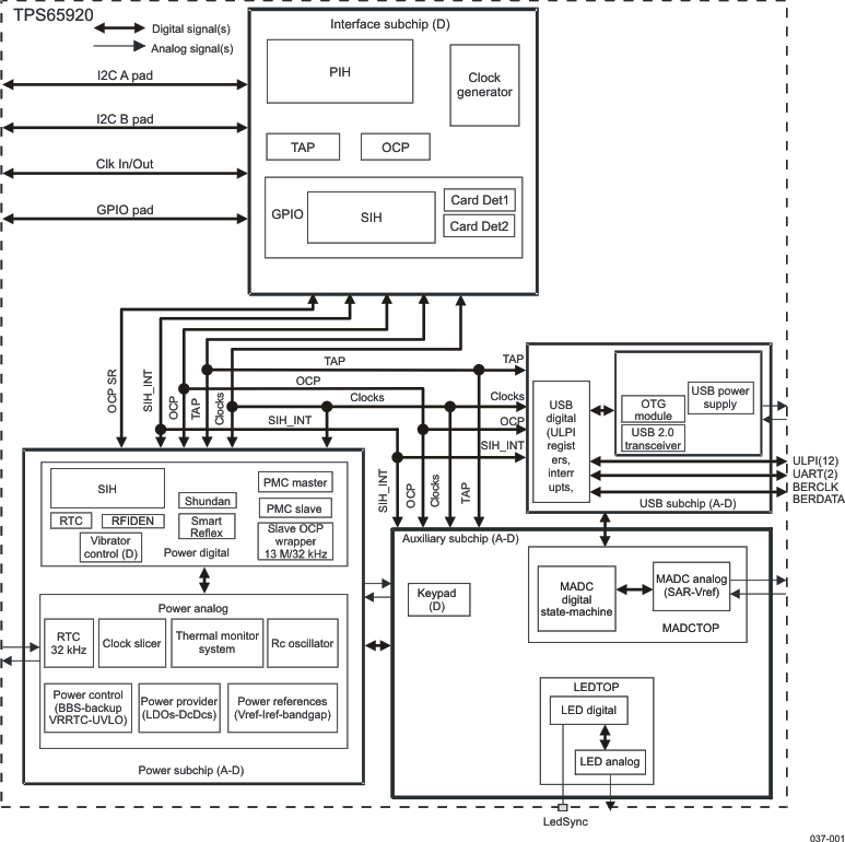
Figure 1-1 TPS65920 Block Diagram