SWCS037I May 2008 – January 2015 TPS65920 , TPS65930
PRODUCTION DATA.
- 1Device Overview
- 2Revision History
- 3Terminal Configuration and Functions
- 4Specifications
-
5Detailed Description
- 5.1
Power Module
- 5.1.1 Power Providers
- 5.1.2 Power References
- 5.1.3 Power Control
- 5.1.4 Power Consumption
- 5.1.5 Power Management
- 5.2 Real-Time Clock and Embedded Power Controller
- 5.3 USB Transceiver
- 5.4 MADC
- 5.5 LED Drivers
- 5.6 Keyboard
- 5.7 Clock Specifications
- 5.8 Debouncing Time
- 5.9 External Components
- 5.1
Power Module
-
6Audio/Voice Module (TPS65930 Device Only)
- 6.1 Audio/Voice Downlink (RX) Module
- 6.2 Audio Uplink (TX) Module
- 7Device and Documentation Support
- 8Mechanical, Packaging, and Orderable Information
Package Options
Mechanical Data (Package|Pins)
- ZCH|139
Thermal pad, mechanical data (Package|Pins)
Orderable Information
5 Detailed Description
5.1 Power Module
This section describes the electrical characteristics of the voltage regulators and timing characteristics of the supplies digitally controlled in the TPS65920 and TPS65930 devices.
Figure 5-1 is the power provider block diagram.
NOTE
For the component values, see Table 5-48.
5.1.1 Power Providers
Table 5-1 summarizes the power providers.
Table 5-1 Summary of the Power Providers
| NAME | USAGE | TYPE | VOLTAGE RANGE (V) | DEFAULT VOLTAGE | MAXIMUM CURRENT |
|---|---|---|---|---|---|
| VAUX2 | External | LDO | 1.3, 1.5, 1.7, 1.8, 1.9, 2.0, 2.1, 2.2, 2.3, 2.4, 2.5, 2.8 | 1.8 V | 100 mA |
| VMMC1 | External | LDO | 1.85, 2.85, 3.0, 3.15 | 3.0 V | 220 mA |
| VPLL1 | External | LDO | 1.0, 1.2, 1.3, 1.8, 2.8, 3.0 | 1.8 V | 40 mA |
| VDAC | External | LDO | 1.2, 1.3, 1.8 | 1.8 V | 70 mA |
| VIO | External | SMPS | 1.8, 1.85 | 1.8 V | 700 mA |
| VDD1 | External | SMPS | 0.6 ... 1.45 | 1.2 V | 1200 mA |
| VDD2 | External | SMPS | 0.6 ... 1.5 | 1.2 V | 600 mA |
| VINTANA1 | Internal | LDO | 1.5 | 1.5 V | 50 mA |
| VINTANA2 | Internal | LDO | 2.5, 2.75 | 2.75 V | 250 mA |
| VINTDIG | Internal | LDO | 1.0, 1.2, 1.3, 1.5 | 1.5 V | 80 mA |
| USBCP | Internal | Charge pump | 5 | 5 V | 100 mA |
| VUSB1V5 | Internal | LDO | 1.5 | 1.5 V | 30 mA |
| VUSB1V8 | Internal | LDO | 1.8 | 1.8 V | 30 mA |
| VUSB3V1 | Internal | LDO | 3.1 | 3.1 V | 15 mA |
| VRRTC | Internal | LDO | 1.5 | 1.5 V | 30 mA |
| VBRTC | Internal | LDO | 1.3 | 1.3 V | 100 μA |
5.1.1.1 VDD1 DC-DC Regulator
5.1.1.1.1 VDD1 DC-DC Regulator Characteristics
The VDD1 DC-DC regulator is a stepdown DC-DC converter with a configurable output voltage. The programming of the output voltage and the characteristics of the DC-DC converter are SmartReflex-compatible. The regulator can be put in sleep mode to reduce its leakage (PFM) or in power-down mode when it is not in use. Table 5-3 describes the regulator characteristics.
Table 5-2 Part Names With Corresponding VDD1 Current Support
| DEVICE NAME | VDD1 CURRENT SUPPORT |
|---|---|
| TPS65920A2ZCH (some bug fixes, see errata) | 1.2 A |
| TPS65920A2ZCHR (some bug fixes, see errata) | 1.2 A |
| TPS65930A2ZCH (some bug fixes, see errata) | 1.2 A |
| TPS65930A2ZCHR (some bug fixes, see errata) | 1.2 A |
Table 5-3 VDD1 DC-DC Regulator Characteristics
| PARAMETER | COMMENTS | MIN | TYP | MAX | UNIT |
|---|---|---|---|---|---|
| Input voltage range | 2.7 | 3.6 | 4.5 | V | |
| Output voltage | 0.6 | 1.45 | V | ||
| Output voltage step | Covering the 0.6-V to 1.45-V range | 12.5 | mV | ||
| Output accuracy(1) | 0.6 V to < 0.8 V | –6% | 6% | ||
| 0.8 V to 1.45 V | –4% | 4% | |||
| Switching frequency | 3.2 | MHz | |||
| Conversion efficiency(2), Figure 5-2 in active mode | IO = 10 mA, sleep | 82% | |||
| 100 mA < IO < 400 mA | 85% | ||||
| 400 mA < IO < 600 mA | 80% | ||||
| 600 mA < IO < 800 mA | 75% | ||||
| Output current | Active mode | 1.2 | A | ||
| Sleep mode | 10 | mA | |||
| Ground current (IQ) | Off at 30°C | 3 | μA | ||
| Sleep, unloaded | 30 | 50 | |||
| Active, unloaded, not switching | 300 | ||||
| Short-circuit current | VIN = VMax | 2.2 | A | ||
| Load regulation | 0 < IO < IMax | 20 | mV | ||
| Transient load regulation(3) | IO = 10 mA to (IMax/2) + 10 mA, Maximum slew rate is IMax/2/100 ns |
–65 | 50 | mV | |
| Line regulation | 10 | mV | |||
| Transient line regulation | 300 mVPP ac input, 10-μs rise and fall time | 10 | mV | ||
| Start-up time | 0.25 | 1 | ms | ||
| Recovery time | From sleep mode to on mode with constant load | <10 | 100 | μs | |
| Slew rate (rising or falling)(4) | 4 | 8 | 16 | mV/μs | |
| Output shunt resistor (pulldown) | 500 | 700 | Ω | ||
| External coil | Value | 0.7 | 1 | 1.3 | μH |
| Data capture record (DCR) | 0.1 | Ω | |||
| Saturation current | 1.8 | A | |||
| External capacitor(5) | Value | 8 | 10 | 12 | μF |
| Equivalent series resistance (ESR) at switching frequency | 0 | 20 | mΩ |
Imax/2 (550 mA) in 100 ns with a ±20% external capacitor accuracy or
Imax/3 (367 mA) in 100 ns with a ±50% external capacitor accuracy
See Table 3-2 for how to connect the VDD1/2 DC-DC converter when it is not in use.
Figure 5-2 shows the efficiency of the VDD1 DC-DC regulator in active mode and sleep mode.
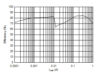 Figure 5-2 VDD1 DC-DC Regulator Efficiency
5.1.1.1.2 External Components and Application Schematics
Figure 5-3 is an application schematic with the external components on the VDD1 DC-DC regulator.
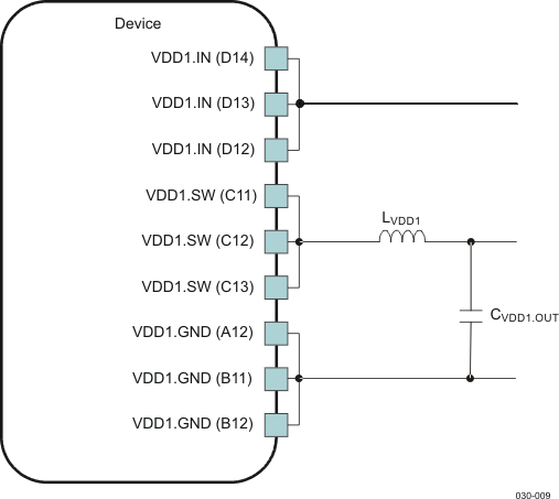 Figure 5-3 VDD1 DC-DC Application Schematic
NOTE
For the component values, see Table 5-48.
5.1.1.2 VDD2 DC-DC Regulator
5.1.1.2.1 VDD2 DC-DC Regulator Characteristics
The VDD2 DC-DC regulator is a programmable output stepdown DC-DC converter with an internal field effect transistor (FET). Like the VDD1 regulator, the VDD2 regulator can be placed in sleep or power-down mode and is SmartReflex-compatible. The VDD2 regulator differs from VDD1 in its current load capability. Table 5-4 describes the regulator characteristics.
Table 5-4 VDD2 DC-DC Regulator Characteristics
| PARAMETER | COMMENTS | MIN | TYP | MAX | UNIT |
|---|---|---|---|---|---|
| Input voltage range | 2.7 | 3.6 | 4.5 | V | |
| Output voltage | 0.6 | 1 | 1.5 | V | |
| Output voltage step | Covering the 0.6-V to 1.45-V range, 1.5 V is a single programmable value |
12.5 | mV | ||
| Output accuracy(1) | 0.6 V to < 0.8 V | –6% | 6% | ||
| 0.8 V to 1.5 V | –4% | 4% | |||
| Switching frequency | 3.2 | MHz | |||
| Conversion efficiency(2), Figure 5-4 in active mode | IO = 10 mA, sleep | 82% | |||
| 100 mA < IO < 300 mA | 85% | ||||
| 300 mA < IO < 500 mA | 80% | ||||
| Output current | Active mode | 600 | mA | ||
| Sleep mode | 10 | mA | |||
| Ground current (IQ) | Off at 30°C | 1 | μA | ||
| Sleep, unloaded | 50 | ||||
| Active, unloaded, not switching | 300 | ||||
| Short-circuit current | VIN = VMax | 1.2 | A | ||
| Load regulation | 0 < IO < IMax | 20 | mV | ||
| Transient load regulation(3) | IO = 10 mA to (IMax/2) + 10 mA, Maximum slew rate is IMax/2/100 ns |
–65 | 50 | mV | |
| Line regulation | 10 | mV | |||
| Transient line regulation | 300 mVPP ac input, 10-μs rise and fall time | 10 | mV | ||
| Output shunt resistor (internal pulldown) | 500 | 700 | Ω | ||
| Start-up time | 0.25 | 1 | ms | ||
| Recovery time | From sleep mode to on mode with constant load | 25 | 100 | μs | |
| Slew rate (rising or falling)(4) | 4 | 8 | 16 | mV/μs | |
| External coil | Value | 0.7 | 1 | 1.3 | μH |
| DCR | 0.1 | Ω | |||
| Saturation current | 900 | mA | |||
| External capacitor(5) | Value | 8 | 10 | 12 | μF |
| ESR at switching frequency | 0 | 20 | mΩ |
Imax/2 (300 mA) in 100 ns with a ±20% external capacitor accuracy or
Imax/3 (200 mA) in 100 ns with a ±50% external capacitor accuracy
See Table 3-2 for how to connect the VDD1/2 DC-DC converter when it is not in use.
Figure 5-4 shows the efficiency of the VDD2 DC-DC regulator in active mode and sleep mode.
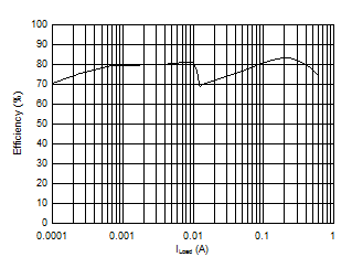 Figure 5-4 VDD2 DC-DC Regulator Efficiency
5.1.1.2.2 External Components and Application Schematics
Figure 5-5 is an application schematic with the external components on the VDD2 DC-DC regulator.
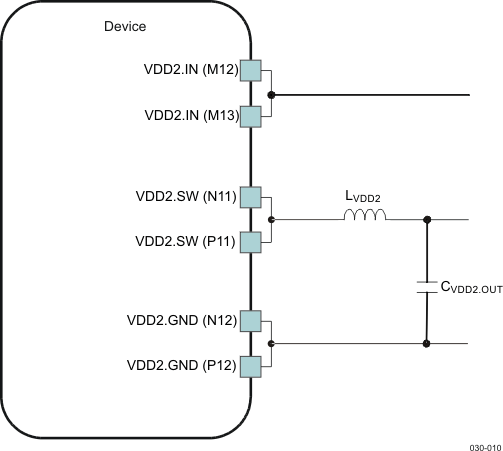 Figure 5-5 VDD2 DC-DC Application Schematic
NOTE
For the component values, see Table 5-48.
5.1.1.3 VIO DC-DC Regulator
5.1.1.3.1 VIO DC-DC Regulator Characteristics
The I/O and memory DC-DC regulator is a 600-mA stepdown DC-DC converter (internal FET) with two output voltage settings. It supplies the memories and all I/O ports in the application and is one of the first power providers to switch on in the power-up sequence. This DC-DC regulator can be placed in sleep or power-down mode; however, care must be taken in the sequencing of this power provider, because numerous ESD blocks are connected to this supply. Table 5-5 describes the regulator characteristics.
Table 5-5 VIO DC-DC Regulator Characteristics
| PARAMETER | COMMENTS | MIN | TYP | MAX | UNIT |
|---|---|---|---|---|---|
| Input voltage range | 2.7 | 3.6 | 4.5 | V | |
| Output voltage(1) | 1.8 1.85 |
V | |||
| Output accuracy (2) | –4% | 4% | |||
| –3% | 3% | ||||
| Switching frequency | 3.2 | MHz | |||
| Conversion efficiency(3)Figure 5-6 in active mode | IO = 10 mA, sleep | 85% | |||
| 100 mA < IO < 400 mA | 85% | ||||
| 400 mA < IO < 600 mA | 80% | ||||
| Output current | On mode | 700 | mA | ||
| Sleep mode | 10 | ||||
| Ground current (IQ) | Off at 30°C | 1 | μA | ||
| Sleep, unloaded | 50 | ||||
| Active, unloaded, not switching | 300 | ||||
| Load transient(4) | 50 | mV | |||
| Line transient | 300 mVPP ac, input rise and fall time 10 μs | 10 | mV | ||
| Start-up time | 0.25 | 1 | ms | ||
| Recovery time | From sleep mode to on mode with constant load | <10 | 100 | μs | |
| Output shunt resistor (internal pulldown) | 500 | 700 | Ω | ||
| External coil | Value | 0.7 | 1 | 1.3 | μH |
| DCR | 0.1 | Ω | |||
| Saturation current | 900 | mA | |||
| External capacitor | Value | 8 | 10 | 12 | μF |
| ESR at switching frequency | 1 | 20 | mΩ |
±3% accuracy is dc accuracy only.
Figure 5-6 shows the efficiency of the VIO DC-DC regulator in active mode and sleep mode.
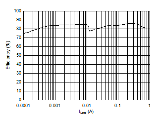 Figure 5-6 VIO DC-DC Regulator Efficiency
Output Voltage = 1.2 V, VBAT = 3.8 V
5.1.1.3.2 External Components and Application Schematics
Figure 5-7 is an application schematic with the external components on the VIO DC-DC regulator.
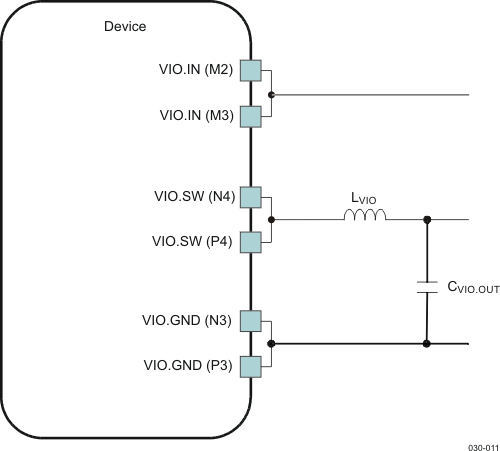 Figure 5-7 VIO DC-DC Application Schematic
NOTE
For the component values, see Table 5-48.
5.1.1.4 VDAC LDO Regulator
The VDAC programmable LDO regulator is a high-PSRR, low-noise linear regulator that powers the host processor dual-video DAC. It is controllable with registers through I2C and can be powered down. Table 5-6 describes the regulator characteristics.
Table 5-6 VDAC LDO Regulator Characteristics
| PARAMETER | TEST CONDITIONS | MIN | TYP | MAX | UNIT | |
|---|---|---|---|---|---|---|
| Output Load Conditions | ||||||
| Filtering capacitor | Connected from VDAC.OUT to analog ground | 0.3 | 1 | 2.7 | μF | |
| Filtering capacitor ESR | 20 | 600 | mΩ | |||
| Electrical Characteristics | ||||||
| VIN | Input voltage | 2.7 | 3.6 | 4.5 | V | |
| VOUT | Output voltage | On mode | 1.164 | 1.2 | 1.236 | V |
| 1.261 | 1.3 | 1.339 | ||||
| 1.746 | 1.8 | 1.854 | ||||
| IOUT | Rated output current | On mode | 70 | mA | ||
| Low-power mode | 5 | |||||
| dc load regulation | On mode: 0 < IO < IMax | 20 | mV | |||
| dc line regulation | On mode, VIN = VINmin to VINmax at IOUT = IOUTmax | 3 | mV | |||
| Turn-on time | IOUT = 0, CL = 1 μF (within 10% of VOUT) | 100 | μs | |||
| Wake-up time | Full load capability | 10 | μs | |||
| Ripple rejection | f < 20 kHz | 65 | dB | |||
| 20 kHz < f < 100 kHz | 45 | |||||
| f = 1 MHz | 40 | |||||
| VIN = VOUT + 1 V, IO = IMax | ||||||
| Output noise | 100 Hz < f < 5 kHz | 400 | nV/√Hz | |||
| 5 kHz < f < 400 kHz | 125 | |||||
| 400 kHz < f < 10 MHz | 50 | |||||
| Ground current | On mode, IOUT = 0 | 150 | μA | |||
| On mode, IOUT = IOUTmax | 350 | |||||
| Low-power mode, IOUT = 0 | 15 | |||||
| Low-power mode, IOUT = 1 mA | 25 | |||||
| Off mode at 55°C | 1 | |||||
| VDO | Dropout voltage | On mode, IOUT = IOUTmax | 250 | mV | ||
| Transient load regulation | ILoad: IMin – IMax
Slew: 60 mA/μs |
–40 | 40 | mV | ||
| Transient line regulation | VIN drops 500 mV Slew: 40 mV/μs |
10 | mV | |||
5.1.1.5 VPLL1 LDO Regulator
The VPLL1 programmable LDO regulator is a high-PSRR, low-noise, linear regulator used for the host processor PLL supply. Table 5-7 describes the regulator characteristics.
Table 5-7 VPLL1 LDO Regulator Characteristics
| PARAMETER | TEST CONDITIONS | MIN | TYP | MAX | UNIT | |
|---|---|---|---|---|---|---|
| Output Load Conditions | ||||||
| Filtering capacitor | Connected from VPLL1.OUT to analog ground | 0.3 | 1 | 2.7 | μF | |
| Filtering capacitor ESR | 20 | 600 | mΩ | |||
| Electrical Characteristics | ||||||
| VIN | Input voltage | 2.7 | 3.6 | 4.5 | V | |
| VOUT | Output voltage | On mode and low-power mode | 0.97 | 1.0 | 1.03 | V |
| 1.164 | 1.2 | 1.236 | ||||
| 1.261 | 1.3 | 1.339 | ||||
| 1.746 | 1.8 | 1.854 | ||||
| 2.716 | 2.8 | 2.884 | ||||
| 2.91 | 3.0 | 3.090 | ||||
| IOUT | Rated output current | On mode | 40 | mA | ||
| Low-power mode | 5 | |||||
| dc load regulation | On mode: 0 < IO < IMax | 20 | mV | |||
| dc line regulation | On mode, VIN = VINmin to VINmax at IOUT = IOUTmax | 3 | mV | |||
| Turn-on time | IOUT = 0, CL = 1 μF (within 10% of VOUT) | 100 | μs | |||
| Wake-up time | Full load capability | 10 | μs | |||
| Ripple rejection | f < 10 kHz | 50 | dB | |||
| 10 kHz < f < 100 kHz | 40 | |||||
| f = 1 MHz | 30 | |||||
| VIN = VOUT + 1 V, IO = IMax | ||||||
| Ground current | On mode, IOUT = 0 | 70 | μA | |||
| On mode, IOUT = IOUTmax | 110 | |||||
| Low-power mode, IOUT = 0 | 15 | |||||
| Low-power mode, IOUT = 1 mA | 16 | |||||
| Off mode at 55°C | 1 | |||||
| VDO | Dropout voltage | On mode, IOUT = IOUTmax | 250 | mV | ||
| Transient load regulation | ILoad: IMin – IMax
Slew: 60 mA/μs |
–40 | 40 | mV | ||
| Transient line regulation | VIN drops 500 mV Slew: 40 mV/μs |
10 | mV | |||
5.1.1.6 VMMC1 LDO Regulator
The VMMC1 LDO regulator is a programmable linear voltage converter that powers the multimedia card (MMC) slot. It includes a discharge resistor and overcurrent protection (short-circuit). This LDO regulator can also be turned off automatically when MMC card extraction is detected. The VMMC1 LDO can be powered through an independent supply other than the battery; for example, a charge pump. In this case, the input from the VMMC1 LDO can be higher than the battery voltage. Table 5-8 describes the regulator characteristics.
Table 5-8 VMMC1 LDO Regulator Characteristics
| PARAMETER | TEST CONDITIONS | MIN | TYP | MAX | UNIT | |
|---|---|---|---|---|---|---|
| Output Load Conditions | ||||||
| Filtering capacitor | Connected from VMMC1.OUT to analog ground | 0.3 | 1 | 2.7 | μF | |
| Filtering capacitor ESR | 20 | 600 | mΩ | |||
| Electrical Characteristics | ||||||
| VIN | Input voltage | 2.7 | 3.6 | 5.5 | V | |
| VOUT | Output voltage | On mode and low-power mode | 1.7945 2.7645 2.91 3.0555 |
1.85 2.85 3.0 3.15 |
1.9055 2.9355 3.09 3.2445 |
V |
| IOUT | Rated output current | On mode Low-power mode |
220 5 |
mA | ||
| dc load regulation | On mode: 0 < IO < IMax | 20 | mV | |||
| dc line regulation | On mode, VIN = VINmin to VINmax at IOUT = IOUTmax | 3 | mV | |||
| Turn-on time | IOUT = 0, CL = 1 μF (within 10% of VOUT) | 100 | μs | |||
| Wake-up time | Full load capability | 10 | μs | |||
| Ripple rejection | f < 10 kHz 10 kHz < f < 100 kHz f = 1 MHz VIN = VOUT + 1 V, IO = IMax |
50 40 25 |
dB | |||
| Ground current | On mode, IOUT = 0 On mode, IOUT = IOUTmax Low-power mode, IOUT = 0 Low-power mode, IOUT = 5 mA Off mode at 55°C |
70 290 17 20 1 |
μA | |||
| VDO | Dropout voltage | On mode, IOUT = IOUTmax | 250 | mV | ||
| Transient load regulation | ILoad: IMin – IMax
Slew: 40 mA/μs |
–40 | 40 | mV | ||
| Transient line regulation | VIN drops 500 mV Slew: 40 mV/μs |
10 | mV | |||
5.1.1.7 VAUX2 LDO Regulator
The VAUX2 general-purpose LDO regulator powers the auxiliary devices. Table 5-9 describes the regulator characteristics.
Table 5-9 VAUX2 LDO Regulator Characteristics
| PARAMETER | TEST CONDITIONS | MIN | TYP | MAX | UNIT | |
|---|---|---|---|---|---|---|
| Output Load Conditions | ||||||
| Filtering capacitor | Connected from VAUX2.OUT to analog ground | 0.3 | 1 | 2.7 | μF | |
| Filtering capacitor ESR | 20 | 600 | mΩ | |||
| Electrical Characteristics | ||||||
| VIN | Input voltage | 2.7 | 3.6 | 4.5 | V | |
| VOUT | Output voltage | On mode and low-power mode | –3% | 1.3 1.5 1.7 1.8 1.9 2.0 2.1 2.2 2.3 2.4 2.5 2.8 |
3% | V |
| IOUT | Rated output current | On mode Low-power mode |
100 5 |
mA | ||
| dc load regulation | On mode: IOUT = IOUTmax to 0 | 20 | mV | |||
| dc line regulation | On mode, VIN = VINmin to VINmax at IOUT = IOUTmax | 3 | mV | |||
| Turn-on time | IOUT = 0, CL = 1 μF (within 10% of VOUT) | 100 | μs | |||
| Wake-up time | Full load capability | 10 | μs | |||
| Ripple rejection | f < 10 kHz 10 kHz < f < 100 kHz f = 1 MHz VIN = VOUT + 1 V, IO = IMax |
50 40 25 |
dB | |||
| Ground current | On mode, IOUT = 0 On mode, IOUT = IOUTmax Low-power mode, IOUT = 0 Low-power mode, IOUT = 5 mA Off mode at 55°C |
70 170 17 20 1 |
μA | |||
| VDO | Dropout voltage | On mode, IOUT = IOUTmax | 250 | mV | ||
| Transient load regulation | ILoad: IMin – IMax
Slew: 40 mA/μs |
–40 | 40 | mV | ||
| Transient line regulation | VIN drops 500 mV Slew: 40 mV/μs |
10 | mV | |||
5.1.1.8 Output Load Conditions
Table 5-10 lists the regulators that power the device, and the output loads associated with them.
Table 5-10 Output Load Conditions
| REGULATOR | PARAMETER | TEST CONDITIONS | MIN | TYP | MAX | UNIT |
|---|---|---|---|---|---|---|
| VINTDIG LDO | Filtering capacitor | Connected from VINTDIG.OUT to analog ground | 0.3 | 1 | 2.7 | μF |
| Filtering capacitor ESR | 20 | 600 | mΩ | |||
| VINTANA1 LDO | Filtering capacitor | Connected from VINTANA1.OUT to analog ground | 0.3 | 1 | 2.7 | μF |
| Filtering capacitor ESR | 20 | 600 | mΩ | |||
| VINTANA2 LDO | Filtering capacitor | Connected from VINTANA2.OUT to analog ground | 0.3 | 1 | 2.7 | μF |
| Filtering capacitor ESR | 20 | 600 | mΩ | |||
| VRUSB_3V1 LDO | Filtering capacitor | Connected from VUSB.3P1 to GND | 0.3 | 1 | 2.7 | μF |
| Filtering capacitor ESR | 0 | 10 | 600 | mΩ | ||
| VRUSB_1V8 LDO | Filtering capacitor | Connected from VINTUSB1P8.OUT to GND | 0.3 | 1 | 2.7 | μF |
| Filtering capacitor ESR | 0 | 10 | 600 | mΩ | ||
| VRUSB_1V5 LDO | Filtering capacitor | Connected from VINTUSB1P5 to GND | 0.3 | 1 | 2.7 | μF |
| Filtering capacitor ESR | 0 | 10 | 600 | mΩ |
5.1.1.9 Charge Pump
The charge pump generates a 4.8-V (nominal) power supply voltage from the battery to the VBUS pin. The input voltage range is 2.7 to 4.5 V for the battery voltage. The charge pump operating frequency is 1 MHz.
The charge pump tolerates 7 V on VBUS when it is in power-down mode. The charge pump integrates a short-circuit current limitation at 450 mA. Table 5-11 lists the charge pump output load conditions.
Table 5-11 Charge Pump Output Load Conditions
| PARAMETER | TEST CONDITIONS | MIN | TYP | MAX | UNIT | |
|---|---|---|---|---|---|---|
| Output Load Conditions | ||||||
| Filtering capacitor | Connected from VBUS to VSSP | 1.41 | 4.7 | 6.5 | μF | |
| Flying capacitor | Connected from CP to CN | 1.32 | 2.2 | 3.08 | μF | |
| Filtering capacitor ESR | 20 | mΩ | ||||
5.1.1.10 USB LDO Short-Circuit Protection Scheme
The short-circuit current for the LDOs and DC-DCs in the TPS65920 and TPS65930 devices is approximately twice the maximum load current. When the output of the block is shorted to ground, the power dissipation can exceed the 1.2-W requirement if no action is taken. A short-circuit protection scheme is included in the TPS65920 and TPS65930 devices to ensure that if the output of an LDO or DC-DC is short-circuited, the power dissipation does not exceed the 1.2-W level.
The three USB LDOs, VRUSB3V1, VRUSB1V8, and VRUSB1V5, are included in this short-circuit protection scheme, which monitors the LDO output voltage at a frequency of 1 Hz and generates an interrupt (sc_it) when a short-circuit is detected.
The scheme compares the LDO output voltage to a reference voltage and detects a short-circuit if the LDO voltage drops below this reference value (0.5 or 0.75 V programmable). In the case of the VRUSB3V1 and VRUSB1V8 LDOs, the reference is compared with a divided down voltage (1.5 V typical).
If a short-circuit is detected on VRUSB3V1, the power subchip FSM switches this LDO to sleep mode.
If a short-circuit is detected on VRUSB1V8 or VRUSB1V5, the power subchip FSM switches off the relevant LDO.
5.1.2 Power References
The bandgap voltage reference is filtered (resistance/capacitance [RC] filter) using an external capacitor connected across the VREF output and an analog ground (REFGND). The VREF voltage is scaled, distributed, and buffered in the device. The bandgap is started in fast mode (not filtered), and is set automatically by the power state-machine in slow mode (filtered, less noisy) when required.
Table 5-12 lists the voltage reference characteristics.
Table 5-12 Voltage Reference Characteristics
| PARAMETER | TEST CONDITIONS | MIN | TYP | MAX | UNIT | |
|---|---|---|---|---|---|---|
| Output Load Condition | ||||||
| Filtering capacitor | Connected from VREF to GNDREF | 0.3 | 1 | 2.7 | μF | |
| Electrical Characteristics | ||||||
| VIN | Input voltage | On mode | 2.7 | 3.6 | 4.5 | V |
| Internal bandgap reference voltage | On mode, measured through TESTV terminal | 1.272 | 1.285 | 1.298 | V | |
| Reference voltage (VREF terminal) | On mode | 0.749 | 0.75 | 0.77 | V | |
| Retention mode reference | On mode | 0.492 | 0.5 | 0.508 | V | |
| IREF NMOS sink | 0.9 | 1 | 1.1 | μA | ||
| Ground current | Bandgap IREF block Preregulator VREF buffer Retention reference buffer |
25 20 15 10 10 |
μA | |||
| Output spot noise | 100 Hz | 1 | μV/√Hz | |||
| A-weighted noise (rms) | 200 | nV (rms) | ||||
| P-weighted noise (rms) | 150 | nV (rms) | ||||
| Integrated noise | 20 to 100 kHz | 2.2 | μV | |||
| IBIAS trim bit LSB | 0.1 | μA | ||||
| Ripple rejection | <1 MHz from VBAT | 60 | dB | |||
| Start-up time | 1 | ms | ||||
5.1.3 Power Control
5.1.3.1 Backup Battery Charger
If the backup battery is rechargeable, it can be recharged from the main battery. A programmable voltage regulator powered by the main battery allows recharging of the backup battery. The backup battery charge must be enabled using a control bit register. Recharging starts when two conditions are met:
- Main battery voltage > backup battery voltage
- Main battery > 3.2 V
The comparators of the backup battery system (BBS) give the two thresholds of the backup battery charge startup. The programmed voltage for the charger gives the end-of-charge threshold. The programmed current for the charger gives the charge current.
Overcharging is prevented by measurement of the backup battery voltage through the GP ADC. Table 5-13 lists the characteristics of the backup battery charger.
Table 5-13 Backup Battery Charger Characteristics
| PARAMETER | TEST CONDITIONS | MIN | TYP | MAX | UNIT |
|---|---|---|---|---|---|
| VBACKUP-to-MADC input attenuation | VBACKUP from 1.8 to 3.3 V | 0.33 | V/V | ||
| Backup battery charging current | VBACKUP = 2.8 V, BBCHEN = 1, BBISEL = 00 | 10 | 25 | 45 | μA |
| VBACKUP = 2.8 V, BBCHEN = 1, BBISEL = 01 | 105 | 150 | 270 | μA | |
| VBACKUP = 2.8 V, BBCHEN = 1, BBISEL = 10 | 350 | 500 | 900 | μA | |
| VBACKUP = 2.8 V, BBCHEN = 1, BBISEL = 11 | 0.7 | 1 | 1.8 | mA | |
| VBACKUP = 0 V, BBCHEN = 1, BBISEL = 00 | 17.5 | 25 | 45 | μA | |
| VBACKUP = 0 V, BBCHEN = 1, BBISEL = 01 | 105 | 150 | 270 | μA | |
| VBACKUP = 0 V, BBCHEN = 1, BBISEL = 10 | 350 | 500 | 900 | μA | |
| VBACKUP = 0 V, BBCHEN = 1, BBISEL = 11 | 0.7 | 1 | 1.8 | mA | |
| End backup battery charging voltage: VBBCHGEND | IVBACKUP = –10 μA, BBSEL = 00 | 2.4 | 2.5 | 2.6 | V |
| IVBACKUP = –10 μA, BBSEL = 01 | 2.9 | 3.0 | 3.1 | V | |
| IVBACKUP = –10 μA, BBSEL = 10 | 3.0 | 3.1 | 3.2 | V | |
| IVBACKUP = –10 μA, BBSEL = 11 | 3.1 | 3.2 | 3.3 | V |
5.1.3.2 Battery Monitoring and Threshold Detection
5.1.3.2.1 Power On/Power Off and Backup Conditions
Table 5-14 lists the threshold levels of the battery.
Table 5-14 Battery Threshold Levels
| PARAMETER | TEST CONDITIONS | MIN | TYP | MAX | UNIT |
|---|---|---|---|---|---|
| Main battery charged threshold VMBCH | Measured on VBAT terminal | 3.1 | 3.2 | 3.3 | V |
| Main battery low threshold VMBLO | VBACKUP = 3.2 V, measured on VBAT terminal (monitored on terminal ONNOFF) | 2.55 | 2.7 | 2.85 | V |
| Main battery high threshold VMBHI | Measured on terminal VBAT, VBACKUP = 0 V Measured on terminal VBAT, VBACKUP = 3.2 V |
2.5 2.5 |
2.65 2.85 |
2.95 2.95 |
V |
| Batteries not present threshold VBNPR | Measured on terminal VBACKUP with VBAT < 2.1 V Measured on terminal VBAT with VBACKUP = 0 V (monitored on terminal VRRTC) |
1.6 1.95 |
1.8 2.1 |
2.0 2.25 |
V |
5.1.3.3 VRRTC LDO Regulator
The VRRTC voltage regulator is a programmable, low dropout, linear voltage regulator supplying (1.5 V) the embedded real-time clock (32.768-kHz oscillator) and dedicated I/Os of the digital host counterpart. The VRRTC regulator is also the supply voltage of the power-management digital state-machine. The VRRTC regulator is supplied from the UPR line, switched on by the main or backup battery, depending on the system state. The VRRTC output is present as long as a valid energy source is present. The VRRTC line is supplied by an LDO when VBAT > 2.7, and a clamp circuit when in backup mode. Table 5-15 describes the regulator characteristics.
Table 5-15 VRRTC LDO Regulator Characteristics
| PARAMETER | TEST CONDITIONS | MIN | TYP | MAX | UNIT | |
|---|---|---|---|---|---|---|
| Output Load Conditions | ||||||
| Filtering capacitor | Connected from VRTC.OUT to analog ground | 0.3 | 1 | 2.7 | μF | |
| Filtering capacitor ESR | 20 | 600 | mΩ | |||
| Electrical Characteristics | ||||||
| VIN | Input voltage | On mode | 2.7 | VBAT | 4.5 | V |
| VOUT | Output voltage | On mode | 1.45 | 1.5 | 1.55 | V |
| IOUT | Rated output current | On mode | 30 | mA | ||
| Sleep mode | 1 | |||||
| DC load regulation | On mode: IOUT = IOUTmax to 0 | 100 | mV | |||
| DC line regulation | On mode, VIN = VINmin to VINmax at IOUT = IOUTmax | 100 | mV | |||
| Turn-on time | IOUT = 0, at VOUT = VOUTfinal ± 3% | 100 | μs | |||
| Wake-up time | On mode from low power to On mode, IOUT = 0, at VOUT = VOUTfinal ± 3% | 100 | μs | |||
| From backup to On mode, IOUT = 0, at VOUT = VOUTfinal ± 3% | 100 | |||||
| Ripple rejection (VRRTC) | f < 10 kHz | 50 | dB | |||
| 10 kHz < f < 100 kHz | 40 | |||||
| f = 1 MHz | 30 | |||||
| VIN = VOUT + 1 V, IO = IMAX | ||||||
| Ground current | On mode, IOUT = 0 | 70 | μA | |||
| On mode, IOUT = IOUTmax | 100 | |||||
| Sleep mode, IOUT = 0 | 10 | |||||
| Sleep mode, IOUT = 1 mA | 11 | |||||
| Off mode | 1 | |||||
| VDO | Dropout voltage(1) | On mode, IOUT = IOUTmax | 250 | mV | ||
| Transient load regulation | ILOAD: IMIN – IMAX
Slew: 40 mA/μs |
–40 | 40 | mV | ||
| Transient line regulation | VIN drops 500 mV Slew: 40 mV/μs |
10 | mV | |||
| Overshoot | Softstart | 3% | ||||
| Pull down resistance | Default in off mode | 250 | 320 | 450 | Ω | |
5.1.4 Power Consumption
Table 5-16 describes the power consumption depending on the use cases.
NOTE
Typical power consumption is obtained in the nominal operating conditions and with the TPS65920 and TPS65930 devices in stand-alone configuration.
Table 5-16 Power Consumption
| MODE | DESCRIPTION | TYPICAL CONSUMPTION | |
|---|---|---|---|
| Backup | Only the RTC date is maintained with a couple of registers in the backup domain. No main source is connected. Consumption is on the backup battery. | VBAT not present | 2.25 * 3.2 = 7.2 μW |
| Wait on | The phone is apparently off for the user, a main battery is present and well-charged. The RTC registers and registers in the backup domain are maintained. The wake-up capabilities (such as the PWRON button) are available. | VBAT = 3.8 V | 64 × 3.8 = 243.2 μW |
| Active no load | The subsystem is powered by the main battery, all supplies are enabled with full current capability, internal reset is released, and the associated processor is running. | VBAT = 3.8 V | 3291 × 3.8 = 12505 μW |
| Sleep no load | The main battery powers the subsystem, selected supplies are enabled but in low-consumption mode, and the associated processor is in low-power mode. | VBAT = 3.8 V | 496 × 3.8 = 1884.4 μW |
Table 5-17 lists the regulator states according to the mode in use.
Table 5-17 Regulator State Depending on Use Case
| REGULATOR | MODE | |||
|---|---|---|---|---|
| BACKUP | WAIT ON | SLEEP NO LOAD | ACTIVE NO LOAD | |
| VAUX2 | OFF | OFF | SLEEP | ON |
| VMMC1 | OFF | OFF | OFF | OFF |
| VPLL1 | OFF | OFF | SLEEP | ON |
| VDAC | OFF | OFF | OFF | OFF |
| VINTANA1 | OFF | OFF | SLEEP | ON |
| VINTANA2 | OFF | OFF | SLEEP | ON |
| VINTDIG | OFF | OFF | SLEEP | ON |
| VIO | OFF | OFF | SLEEP | ON |
| VDD1 | OFF | OFF | SLEEP | ON |
| VDD2 | OFF | OFF | SLEEP | ON |
| VUSB_1V5 | OFF | OFF | OFF | OFF |
| VUSB_1V8 | OFF | OFF | OFF | OFF |
| VUSB_3V1 | OFF | OFF | SLEEP | SLEEP |
5.1.5 Power Management
5.1.5.1 Boot Modes
Table 5-18 lists the modes corresponding to BOOT0–BOOT1.
Table 5-18 BOOT Mode Description
| NAME | DESCRIPTION | BOOT0 | BOOT1 |
|---|---|---|---|
| Reserved | 0 | 0 | |
| MC027 | Master_C027_Generic 01 | 0 | 1 |
| MC021 | Master_C021_Generic 10 | 1 | 0 |
| SC021 | Slave_C021_Generic 11 | 1 | 1 |
5.1.5.2 Process Modes
This parameter defines:
- The boot voltage for the host core
- The boot sequence associated with the process
- The dynamic voltage and frequency scaling (DVFS) protocol associated with the process
5.1.5.2.1 MC021 Mode
Table 5-19 lists the characteristics of MC021 mode.
Table 5-19 MC021 Mode
| Boot core voltage | 1.2 V |
| Power sequence | VIO followed by VPLL1, VDD2, VDD1 |
| DVFS protocol | SmartReflex IF (I2C HS) |
5.1.5.3 Power-On Sequence
5.1.5.3.1 Timing Before Sequence_Start
Sequence_Start is a symbolic internal signal to ease the description of the power sequences. It occurs according to the events shown in Figure 5-8.
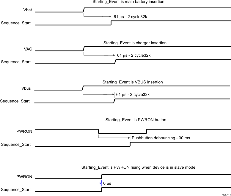 Figure 5-8 Timing Before Sequence Start
5.1.5.3.2 Power-On Sequence
Figure 5-9 describes the timing and control that must occur in the OMAP3 mode. Sequence_Start is a symbolic internal signal to ease the description of the power sequences. It occurs according to the events shown in Figure 5-8.
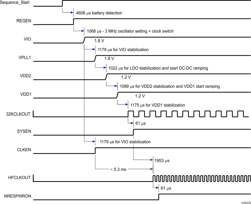 Figure 5-9 Timings–Power On in OMAP3 Mode
5.1.5.3.3 Power On in Slave_C021 Mode
Figure 5-10 describes the timing and control that must occur in the Slave_C021 mode. Sequence_Start is a symbolic internal signal to ease the description of the power sequences and occurs according to the different events detailed in Figure 5-8.
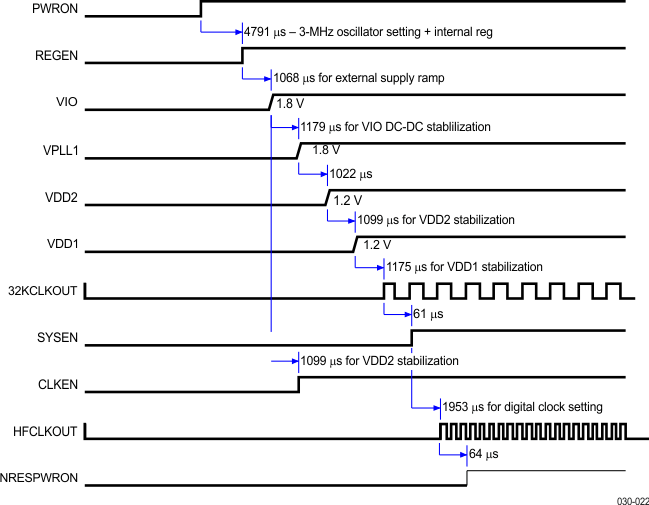 Figure 5-10 Timings—Power On in Slave_C021 Mode
5.1.5.4 Power-Off Sequence
This section describes the signal behavior required to power down the system.
5.1.5.4.1 Power-Off Sequence
Figure 5-11 shows the timing and control that occur during the power-off sequence in master modes.
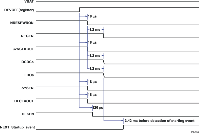
NOTE:
All of these timings are typical values with the default setup (depending on the resynchronization between power domains, state machinery priority, etc.).Because of the internal frequency used by Power STM switching from 3 to 1.5 MHz when the HF clock value is 19.2 MHz, if the HF clock value is not 19.2 MHz (with HFCLK_FREQ bit field values set accordingly in the CFG_BOOT register), the delay between DEVOFF and NRESPWRON/CLK32KOUT/SYSEN/HFCLKOUT is divided by two (approximately 9 μs).
The DEVOFF event is PWRON falling edge in slave mode and DEVOFF internal register write in master mode.
5.2 Real-Time Clock and Embedded Power Controller
The TPS65930 and TPS65920 devices contain an RTC to provide clock and timekeeping functions and an EPC to provide battery supervision and control.
5.2.1 RTC
The RTC provides the following basic functions:
- Time information (seconds/minutes/hours) directly in binary-coded decimal (BCD) code
- Calendar information (day/month/year/day of the week) directly in BCD code
- Interrupt generation periodically (1 second/1 minute/1 hour/1 day) or at a precise time (alarm function)
- 32-kHz oscillator drift compensation and time correction
- Alarm-triggered system wake-up event
5.2.1.1 Backup Battery
The TPS65030 and TPS65920 devicesdevice implement a backup mode in which a backup battery can keep the RTC running to maintain clock and time information even if the main supply is not present. If the backup battery is rechargeable, the device also provides a backup battery charger so it can be recharged when the main battery supply is present.
The backup domain powers the following:
- Internal 32.768-kHz crystal oscillator
- RTC
- Eight general-purpose (GP) storage registers
- Backup domain low-power regulator (VBRTC)
5.2.2 EPC
The EPC provides five system states for optimal power use by the system, as listed in Table 5-20.
Table 5-20 System States
| SYSTEM STATE | DESCRIPTION |
|---|---|
| NO SUPPLY | The system is not powered by any battery. |
| BACKUP | The system is powered only with the backup battery and maintains only the VBRTC supply. |
| WAIT-ON | The system is powered by the main battery and maintains only the VRRTC supply. It can accept switch-on requests. |
| ACTIVE | The system is powered by the main battery; all supplies can be enabled with full current capability. |
| SLEEP | The main battery powers the system; selected supplies are enabled, but in low consumption mode. |
Three categories of events can trigger state transitions:
- Hardware events: Supply/battery insertion, wake-up requests, USB plug, and RTC alarm
- Software events: Switch-off commands, switch-on commands, and sleep on commands
- Monitoring events: Supply/battery level check, main battery removal, main battery fail, and thermal shutdown
5.3 USB Transceiver
The TPS65920/TPS65930 device includes a USB OTG transceiver with the CEA carkit interface that supports USB 480 Mbps HS, 12 Mbps full-speed (FS), and USB 1.5 Mbps low-speed (LS) through a 4-pin ULPI.
The carkit block ensures the interface between the phone and a carkit device. The TPS65920/TPS65930 USB supports the CEA carkit standard.
Figure 5-12 is a block diagram of the USB 2.0 physical layer (PHY).
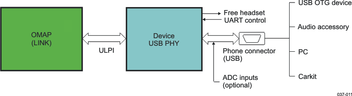 Figure 5-12 USB 2.0 PHY Block Diagram
5.3.1 Features
The device has a USB OTG carkit transceiver that allows system implementation that complies with the following specifications:
- Universal Serial Bus 2.0 Specification
- On-The-Go Supplement to the USB 2.0 Specification
- CEA-2011: OTG Transceiver Interface Specification
- CEA-936A: Mini-USB Analog Carkit Specification
- UTMI+ Low Pin Interface Specification
The features of the individual specifications are:
-
Universal Serial Bus 2.0 Specification (hereafter referred to as the USB 2.0 specification):
- 5-V-tolerant data line at HS/FS, FS-only, and LS-only transmission rates
- 7-V-tolerant video bus (VBUS) line
- Integrated data line serial termination resistors (factory-trimmed)
- Integrated data line pullup and pulldown resistors
- On-chip 480-MHz phase-locked loop (PLL) from the internal system clock (19.2, 26, and 38.4 MHz)
- Synchronization (SYNC)/end-of-period (EOP) generation and checking
- Data and clock recovery from the USB stream
- Bit-stuffing/unstuffing and error detection
- Resume signaling, wakeup, and suspend detection
- USB 2.0 test modes
-
On-The-Go Supplement to the USB 2.0 Specification (hereafter referred to as the OTG supplement to the USB 2.0 specification):
- 3-pin LS/FS serial mode (DAT_SE0)
- 4-pin LS/FS serial mode (VP_VM)
-
CEA-936A: Mini-USB Analog Carkit Interface Specification:
- 5-pin CEA mini-USB analog carkit interface
- UART signaling
- Audio (mono/stereo) signaling
- UART transactions during audio signaling
- Basic and smart 4-wire/5-wire carkit, chargers, and accessories
- ID CEA resistor comparators
-
UTMI+ Low Pin Interface Specification (hereafter referred to as the ULPI specification):
- 12-pin ULPI with 8-pin parallel data for USB signaling and register access
- 60-MHz clock generation
- Register mapping
Figure 5-13 is the USB system application schematic.
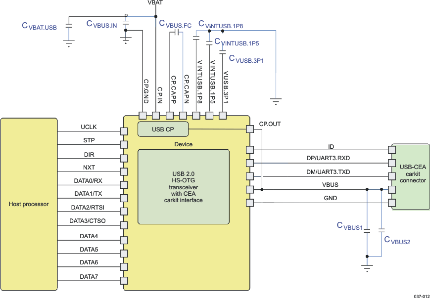 Figure 5-13 USB System Application Schematic
NOTE
For the component values, see Table 5-48.
5.3.2 HS USB Port Timing
The ULPI interface supports an 8-bit data bus and the internal clock mode. The 4-bit data bus and the external clock mode are not supported.
The HS functional mode supports an operating rate of 480 Mbps.
Table 5-21 and Table 5-22 assume testing over the recommended operating conditions (see Figure 5-14).
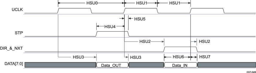 Figure 5-14 HS-USB Interface—Transmit and Receive Modes (ULPI 8-bit)
NOTE
ULPI data [7:0] lines are set to 1 after USB PHY power up, and before the clock signal is stable.
The input timing requirements are given by considering a rising or falling time of 1 ns (see Table 5-21).
Table 5-21 HS-USB Interface Timing Requirements
| NOTATION | PARAMETER | MIN | MAX | UNIT | |
|---|---|---|---|---|---|
| HSU4 | ts(STPV-CLKH) | Setup time, STP valid before UCLK rising edge | 6 | ns | |
| HSU5 | th(CLKH-STPIV) | Hold time, STP valid after UCLK rising edge | 0 | ns | |
| HSU6 | ts(DATAV-CLKH) | Setup time, DATA[0:7] valid before UCLK rising edge | 6 | ns | |
| HSU7 | th(CLKH-DATIV) | Hold time, DATA[0:7] valid after UCLK rising edge | 0 | ns | |
Table 5-22 lists the HS-USB interface switching requirements.
Table 5-22 HS-USB Interface Switching Requirements(1)
| NOTATION | PARAMETER(1) | MIN | TYP | MAX | UNIT | ||
|---|---|---|---|---|---|---|---|
| HSU0 | fp(CLK) | UCLK clock frequency | Steady state | 58.42 | 60 | 61.67 | MHz |
| HSU1 | tW(CLK) | UCLK duty cycle | Steady state | 48.3% | 50% | 51.7% | |
| HSU2 | td(CLKH-DIR) | Delay time, UCLK rising edge to DIR transition | Steady state | 0 | 9 | ns | |
| td(CLKH-NXTV) | Delay time, UCLK rising edge to NXT transition | Steady state | 0 | 9 | ns | ||
| HSU3 | td(CLKH-DATV) | Delay time, UCLK rising edge to DATA[0:7] transition | Steady state | 0 | 9 | ns | |
The capacitive load for the CLK port is 6 pF (rising and falling time is 1 ns).
The HS-USB interface has only one state: the steady state.
5.3.3 USB-CEA Carkit Port Timing
This mode allows the link for communication through the USB PHY to a remote carkit in CEA audio + data during audio (DDA) mode as defined in the CEA-936A specification. In this mode, the ULPI data bus is redefined as a 2-pin UART interface, which exchanges data through a direct access to the FS/LS analog transmitter and receiver.
UART data are sent and received on the USB D+/D– pads. D+/D– are also used in this mode to carry audio I/O signals.
Table 5-23 assumes testing over the recommended operating conditions (see the CEA-936A specification).
Table 5-23 USB-CEA Carkit Interface Timing Parameters
| PARAMETER | MIN | MAX | UNIT | |
|---|---|---|---|---|
| tPH_DP_CON | Phone D+ connect time | 100 | ms | |
| tCR_DP_CON | Carkit D+ connect time | 150 | 300 | ms |
| tPH_DM_CON | Phone D– connect time | 10 | ms | |
| tPH_CMD_DLY | Phone command delay | 2 | ms | |
| tPH_MONO_ACK | Phone mono acknowledge | 10 | ms | |
| tPH_DISC_DET | Phone D+ disconnect time | 150 | ms | |
| tCR_DISC_DET | Carkit D– disconnect detect | 50 | 150 | ms |
| tPH_AUD_BIAS | Phone audio bias | 1 | ms | |
| tCR_AUD_DET | Carkit audio detect | 400 | 800 | μs |
| tCR_UART_DET | Carkit UART detect (data-during-audio enabled) | 700 | 1200 | ns |
| tPH_STLO_DET | Phone stereo D+ low detect | 30 | 100 | ms |
| tPH_PLS_POS | Phone D– interrupt pulse width | 200 | 600 | ns |
| tCR_PLS_NEG | Carkit D+ interrupt pulse width | 200 | 600 | ns |
| tDAT_AUD_POL | Data-during-audio polarity | 20 | 60 | ms |
| tACC_COL_DET | Accessory ID collision detect | 2 | 3 | ms |
| tACC_INT_PW | Accessory ID interrupt pulse width | 200 | 400 | μs |
| tACC_INT_WAIT | Accessory ID interrupt wait time | 10 | 15 | ms |
| tACC_CMD_WAIT | Accessory ID command wait time | 0 | ms | |
| tPH_INT_PW | Phone ID interrupt pulse width | 4 | 8 | ms |
| tPH_INT_WAIT | Phone ID interrupt wait time | 4 | 8 | ms |
| tPH_CMD_WAIT | Phone ID command wait time | 0 | ms | |
| tPH_UART_RPT | Phone command repeat time | 50 | ms | |
| tCR_UART_RSP | Carkit UART response | 30 | ms | |
| tCR_INT_RPT | Carkit interrupt repeat time | 50 | ms | |
| fUART_DFLT | Default UART signaling rate (typical rate) | 9600 | bps | |
Figure 5-15 shows the USB-CEA carkit UART data flow.
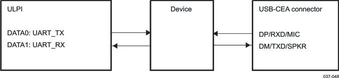 Figure 5-15 USB-CEA Carkit UART Data Flow
Table 5-24 lists the USB-CEA carkit UART timings.
Table 5-24 USB-CEA Carkit UART Timings
| NOTATION | PARAMETER | MIN | MAX | UNIT | ||
|---|---|---|---|---|---|---|
| CK1 | td(UART_TXH-DM) | Delay time, UART_TX rising edge to DM transition | 4.0 | 11 | ns | |
| CK2 | td(UART_TXL-DM) | Delay time, UART_TX falling edge to DM transition | 4.0 | 11 | ns | |
| CK3 | td(DPH-UART_RX) | Delay time, DP rising edge to UART_RX transition | At 38.4 MHz | 205 | 234 | ns |
| At 19.2 MHz | 310 | 364 | ||||
| CK4 | td(DPL-UART_RX) | Delay time, DP falling edge to UART_RX transition | At 38.4 MHz | 205 | 234 | ns |
| At 19.2 MHz | 310 | 364 | ||||
Figure 5-16 shows the USB-CEA carkit UART timings.
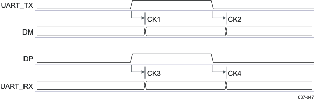 Figure 5-16 USB-CEA Carkit UART Timings
5.3.4 PHY Electrical Characteristics
The PHY is the physical signaling layer of the USB 2.0. It contains the drivers and receivers for physical data and protocol signaling on the DP and DM lines.
The PHY interfaces with the USB controller through the UTMI.
The transmitters and receivers in the PHY are of two main classes:
- FS and LS transceivers (legacy USB1.x transceivers)
- HS transceivers
To bias the transistors and run the logic, the PHY also contains reference generation circuitry which consists of:
- A DPLL that does a frequency multiplication to achieve the 480-MHz low-jitter lock necessary for USB, and the clock required for the switched capacitor resistance block
- A switched capacitor resistance block that replicates an external resistor on chip
Built-in pullup and pulldown resistors are used as part of the protocol signaling.
The PHY also contains circuitry that protects it from an accidental 5-V short on the DP and DM lines and from 8-kV IEC ESD strikes.
5.3.4.1 HS Differential Receiver
The HS receiver consists of the following blocks:
- A differential input comparator to receive the serial data
- A squelch detector to qualify the received data
- An oversampler-based clock data recovery scheme followed by a nonreturn to zero inverted (NRZI) decoder, bit unstuffing, and serial-to-parallel converter to generate the UTMI DATAOUT
Table 5-25 lists the characteristics of the HS differential receiver.
Table 5-25 HS Differential Receiver
| PARAMETER | COMMENTS | MIN | TYP | MAX | UNIT | |
|---|---|---|---|---|---|---|
| Input Levels for HS | ||||||
| HS squelch detection threshold | VHSSQ | (Differential signal amplitude) | 100 | 125 | 150 | mV |
| HS disconnect detection threshold | VHSDSC | (Differential signal amplitude) | 525 | 600 | 625 | mV |
| HS data signaling common mode voltage range | VHSCM | –50 | 200 | 500 | mV | |
| HS differential input sensitivity | VDIHS | (Differential signal amplitude) | –100 | 100 | mV | |
| Input Impedance for HS | ||||||
| Internal specification for input capacitance | CHSLOAD | 11 | pF | |||
| Internal CHSLOAD DP/DM matching | CHSLOADM | 0.2 | pF | |||
| External Components With the Total Budget Combined (without USB cable load) | ||||||
| External capacitance on DP or DM | 2 | pF | ||||
| External series resistance on DP or DM | 1 | Ω | ||||
5.3.4.2 HS Differential Transmitter
The HS transmitter is always operated on the UTMI parallel interface. The parallel data on the interface is serialized, bit stuffed, NRZI encoded, and transmitted as a dc output current on DP or DM, depending on the data. Each line has an effective 22.5-Ω load to ground, which generates the voltage levels for signaling.
A disconnect detector is also part of the HS transmitter. A disconnect on the far end of the cable causes the impedance seen by the transmitter to double, thereby doubling the differential amplitude seen on the DP/DM lines.
Table 5-26 lists the characteristics of the HS differential transmitter.
Table 5-26 HS Differential Transmitter
| PARAMETER | COMMENTS | MIN | TYP | MAX | UNIT | |
|---|---|---|---|---|---|---|
| Output Levels for HS | ||||||
| HS TX idle level | VHSOI | Absolute voltage DP/DM – internal/external 45 Ω | –10 | 0 | 10 | mV |
| HS TX data signaling high | VHSOH | Absolute voltage DP/DM – internal/external 45 Ω | 360 | 400 | 440 | mV |
| HS data signaling low | VHSOL | –10 | 0 | 10 | mV | |
| Chirp J level | VCHIRPJ | Differential voltage | 700 | 800 | 1100 | mV |
| Chirp K level | VCHIRPK | Differential voltage | –900 | –800 | –500 | mV |
| HS TX disconnect threshold | VDISCOUT | Absolute voltage DP/DM – no external 45 Ω | 700 | mV | ||
| Driver Characteristics | ||||||
| Rise time | tHSR | (10%–90%) | 500 | ps | ||
| Fall time | tHSF | (10%–90%) | 500 | ps | ||
| Driver output resistance | ZHSDRV | Also serves as HS termination | 40.5 | 45 | 49.5 | Ω |
5.3.4.3 CEA/UART Driver
Table 5-27 lists the characteristics of the CEA/UART driver.
Table 5-27 CEA/UART Driver
| PARAMETER | COMMENTS | MIN | TYP | MAX | UNIT | |
|---|---|---|---|---|---|---|
| UART Driver CEA | ||||||
| Phone UART edge rates | tPH_UART_EDGE | DP_PULLDOWN asserted | 1 | μs | ||
| Serial interface output high | VOH_SER | ISOURCE = 4 mA | 2.4 | 3.3 | 3.6 | V |
| Serial interface output low | VOL_SER | ISINK = –4 mA | 0 | 0.1 | 0.4 | V |
| Carkit Pulse Driver | ||||||
| Pulse match tolerance | QPLS_MTCH | ZCR_SPKR_IN = 60 kΩ at f = 1 kHz | 5% | |||
| Phone D– interrupt pulse width | tPH_PLS_POS | ZCR_SPKR_IN = 60 kΩ at f = 1 kHz | 200 | 600 | ns | |
| Phone positive pulse voltage | VPH_PLS_POS | ZCR_SPKR_IN = 60 kΩ at f = 1 kHz | 2.8 | 3.6 | V | |
5.3.4.4 Pullup/Pulldown Resistors
Table 5-28 lists the characteristics of pullup/pulldown resistors.
Table 5-28 Pullup/Pulldown Resistors
| PARAMETER | COMMENTS | MIN | TYP | MAX | UNIT | |
|---|---|---|---|---|---|---|
| Pullup Resistors | ||||||
| Bus pullup resistor on upstream port (idle bus) | RPUI | Bus idle | 0.9 | 1.1 | 1.575 | kΩ |
| Bus pullup resistor on upstream port (receiving) | RPUA | Bus driven/driver outputs unloaded | 1.425 | 2.2 | 3.09 | |
| High (floating) | VIHZ | Pullups/pulldowns on DP and DM lines | 2.7 | 3.6 | V | |
| Phone D+ pullup voltage | VPH_DP_UP | Driver outputs unloaded | 3 | 3.3 | 3.6 | V |
| Pulldown Resistors | ||||||
| Phone D+/– pulldown | RPH_DP_DWN | Driver outputs unloaded | 14.25 | 18 | 24.8 | kΩ |
| RPH_DM_DWN | ||||||
| High (floating) | VIHZ | Pullups/pulldowns on DP and DM lines | 2.7 | 3.6 | V | |
| D+/– Data Line | ||||||
| Upstream facing port | CINUB | [1.0] | 22 | 75 | pF | |
| OTG device leakage | VOTG_DATA_LKG | [2] | 0.342 | V | ||
| Input impedance exclusive of pullup/pulldown(1) | ZINP | Driver outputs unloaded (waiver from USB.ORG Standard Committee) | 80 | 120 | kΩ | |
5.3.5 OTG Electrical Characteristics
The OTG block integrates three main functions:
- The USB plug detection function on VBUS and ID
- The ID resistor detection
- The VBUS level detection
5.3.5.1 OTG VBUS Electrical Characteristics
Table 5-29 lists the electrical characteristics of the OTG VBUS.
Table 5-29 OTG VBUS Electrical Characteristics
| PARAMETER | COMMENTS | MIN | TYP | MAX | UNIT | |
|---|---|---|---|---|---|---|
| VBUS Wake-Up Comparator | ||||||
| VBUS wake-up delay | DELVBUS_WK_UP | 15 | μs | |||
| VBUS wake-up threshold | VVBUS_WK_UP | 0.5 | 0.6 | 0.7 | V | |
| VBUS Comparators | ||||||
| A-device session valid | VA_SESS_VLD | 0.8 | 1.1 | 1.4 | V | |
| A-device VBUS valid | VA_VBUS_VLD | 4.4 | 4.5 | 4.6 | V | |
| B-device session end | VB_SESS_END | 0.2 | 0.5 | 0.8 | V | |
| B-device session valid | VB_SESS_VLD | 2.1 | 2.4 | 2.7 | V | |
| VBUS Line | ||||||
| A-device VBUS input impedance to ground | RA_BUS_IN | SRP (VBUS pulsing) capable A-device not driving VBUS | 100 | kΩ | ||
| B-device VBUS SRP pulldown | RB_SRP_DWN | 5.25 V/8 mA, pullup voltage = 3 V | 0.656 | 10 | kΩ | |
| B-device VBUS SRP pullup | RB_SRP_UP | (5.25 V – 3 V)/8 mA, pullup voltage = 3 V | 0.281 | 1 | 2 | kΩ |
| B-device VBUS SRP rise time maximum for OTG-A communication | tRISE_SRP_UP_Max | 0 to 2.1 V with < 13 μF load | 36 | ms | ||
| B-device VBUS SRP rise time minimum for standard host connection | tRISE_SRP_UP_Min | 0.8 to 2.0 V with > 97 μF load | 60 | ms | ||
| VBUS line maximum voltage | If VBUS_CHRG bit is low | 7 | V | |||
5.3.5.2 OTG ID Electrical Characteristics
Table 5-30 lists the electrical characteristics of OTG ID.
Table 5-30 OTG ID Electrical Characteristics
| PARAMETER | COMMENTS | MIN | TYP | MAX | UNIT | |
|---|---|---|---|---|---|---|
| ID Wake-Up Comparator | ||||||
| ID wake-up comparator | RID_WK_UP | Wake-up when ID shorted to ground through a resistor lower than 445 kΩ (±1%) | 445 | kΩ | ||
| ID Comparators — ID External Resistor Specifications | ||||||
| ID ground comparator | RID_GND | ID_GND interrupt when ID shorted to ground through a resistor lower than 10 Ω | 0 | 5 | 10 | Ω |
| ID 100k comparators | RID_100K | ID_100K interrupt when 102 kΩ (1%) resistor plugged in | 101 | 102 | 103 | kΩ |
| ID 200k comparators | RID_200K | ID_200K interrupt when 200 kΩ (1%) resistor plugged in | 198 | 200 | 202 | kΩ |
| ID 440k comparators | RID_440K | ID_440K interrupt when 440 kΩ (1%) resistor plugged in | 435 | 440 | 445 | kΩ |
| ID Float comparator | RID_FLOAT | ID_FLOAT interrupt when ID shorted to ground through a resistor higher than 560 kΩ | 1400 | kΩ | ||
| ID Line | ||||||
| Phone ID pullup to VPH_ID_UP | RPH_ID_UP | ID unloaded (VRUSB) | 70 | 200 | 286 | kΩ |
| Phone ID pullup voltage | VPH_ID_UP | Connected to VRUSB | 2.5 | 3.2 | V | |
| ID line maximum voltage | 5.25 | V | ||||
5.4 MADC
5.4.1 General Description
The TPS65920/TPS65930 device provides the MADC resource to the host processors in the system (hardware and software conversion modes).
The MADC generates interrupt signals to the host processors. Interrupts are handled primarily by the MADC internal secondary interrupt handler and secondly at the upper level (outside the MADC) by the TPS65920/TPS65930 interrupt primary handler.
5.4.2 MADC Electrical Characteristics
Table 5-31 lists the electrical characteristics of the MADC.
Table 5-31 MADC Electrical Characteristics
| PARAMETER | CONDITIONS | MIN | TYP | MAX | UNIT |
|---|---|---|---|---|---|
| Resolution | 10 | Bit | |||
| ADIN2 input dynamic range for external input | 0 | 2.5 | V | ||
| MADC voltage reference | 1.5 | V | |||
| ADIN0 differential nonlinearity | –1 | 1 | LSB | ||
| ADIN0 integral nonlinearity | Best fitting | –2 | 2 | LSB | |
| Integral nonlinearity for ADIN2 | Best fitting for codes 230 to maximum | –2 | 2 | LSB | |
| Best fitting considering offset of 25 LSB | –3.75 | 3.75 | LSB | ||
| Offset | Best fitting | –28.5 | 28.5 | mV | |
| Input bias | 1 | μA | |||
| Input capacitor CBANK | 10 | pF | |||
| Maximum source input resistance Rs (for all 16 internal or external inputs) | 100 | kΩ | |||
| Input current leakage (for all 16 internal or external inputs) | 1 | μA |
5.4.3 Channel Voltage Input Range
Table 5-32 lists the analog input voltage minimum and maximum values.
Table 5-32 Analog Input Voltage Range
| CHANNEL | MIN | TYP | MAX | UNIT | PRESCALER |
|---|---|---|---|---|---|
| ADIN0: General-purpose input | 0 | 1.5 | V | No prescaler DC current source for battery identification through external resistor (10 μA typical) |
|
| ADIN2: General-purpose input(1) | 0 | 2.5 | V | Prescaler in the MADC to be in range 0 to >1.5 V |
5.4.3.1 Sequence Conversion Time (Real-Time or Nonaborted Asynchronous)
Table 5-33 lists the sequence conversion timing characteristics.
Table 5-33 Sequence Conversion Timing Characteristics
| PARAMETER | COMMENTS | MIN | TYP | MAX | UNIT |
|---|---|---|---|---|---|
| F | Running frequency | 1 | MHz | ||
| T = 1/F | Clock period | 1 | μs | ||
| N | Number of analog inputs to convert in a single sequence | 0 | 2 | ||
| Tstart | SW1, SW2, or USB asynchronous request or real-time STARTADC request | 3 | 4 | μs | |
| Tsettling time | Settling time to wait before sampling a stable analog input (capacitor bank charge time) | 5 | 12 | 20 | μs |
| Tsettling is calculated from the max((Rs + Ron)*Cbank) of the two possible input sources (internal or external). Ron is the resistance of the selection analog input switches (5 kΩ). This time is software-programmable by the open-core protocol (OCP) register. | |||||
| Tstartsar | The successive approximation registers ADC start time | 1 | μs | ||
| Tadc time | The successive approximation registers ADC conversion time | 10 | μs | ||
| Tcapture time | Tcapture time is the conversion result capture time. | 2 | μs | ||
| Tstop | 1 | 2 | μs | ||
| Full-conversion sequence time | One channel (N = 1)(1) | 22 | 39 | μs | |
| Both channels(1) | 352 | 624 | |||
| Conversion sequence time | Without Tstart and Tstop: One channel (N = 1)(1) | 18 | 33 | μs | |
| Without Tstart and Tstop: Both channels(1) | 288 | 528 | |||
| STARTADC pulse duration | STARTADC period is T. | 0.33 | 24 | μs |
Table 5-33 is illustrated in Figure 5-17, which is a conversion sequence general timing diagram. The Busy parameter indicates that a conversion sequence is running, and the channel N result register parameter corresponds to the result register of the RT/GP selected channel.
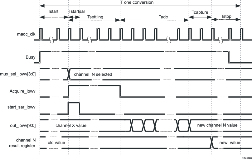 Figure 5-17 Conversion Sequence General Timing Diagram
5.5 LED Drivers
5.5.1 General Description
Two arrays of parallel LEDs are driven (dedicated for the phone light). The parallel LEDs are supplied by VBAT, and the external resistor value is given for each LED. The TPS65920/TPS65930 device supports two open-drain LED drivers for the keypad backlight, having drain connections tolerant of the main battery voltage.
Figure 5-18 is the LED driver block diagram. Table 5-34 lists the electrical characteristics of the LED driver.
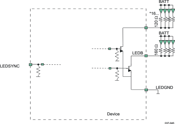 Figure 5-18 LED Driver Block Diagram
NOTE
For the component values, see Table 5-48.
Table 5-34 LED Driver Electrical Characteristics
| PARAMETER | CONDITIONS | MIN | TYP | MAX | UNIT |
|---|---|---|---|---|---|
| SW On resistance | IO = 160 mA | 3 | 4 | Ω | |
| IO = 60 mA | 10 | 12 |
5.6 Keyboard
5.6.1 Keyboard Connection
The keyboard is connected to the chip using:
- KBR (5 :0) input pins for row lines
- KBC (5 :0) output pins for column lines
Figure 5-19 shows the keyboard connection.
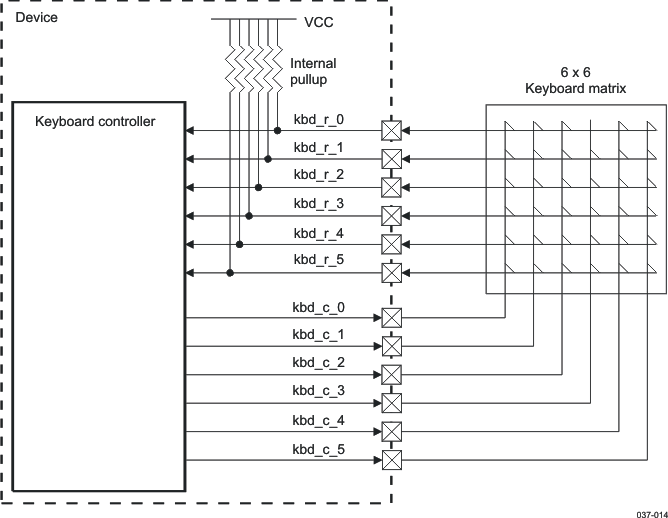 Figure 5-19 Keyboard Connection
When a key button of the keyboard matrix is pressed, the corresponding row and column lines are shorted together. To allow key press detection, all input pins (KBR) are pulled up to VCC and all output pins (KBC) are driven to a low level.
Any action on a button generates an interrupt to the sequencer.
The decoding sequence is written to allow detection of simultaneous press actions on several key buttons.
The keyboard interface can be used with a smaller keyboard area than 6 × 6. To use a 3 × 3 keyboard, KBR(4) and KBR(5) must be tied high to prevent any scanning process distribution.
5.7 Clock Specifications
The TPS65920/TPS65930 device includes several I/O clock pins. The TPS65920/TPS65930 device has two sources of high-stability clock signals: the external high-frequency clock (HFCLKIN) input and an onboard 32-kHz oscillator (an external 32-kHz signal can be provided). Figure 5-20 is the clock overview.
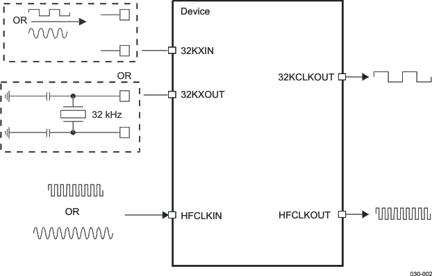 Figure 5-20 Clock Overview
5.7.1 Clock Features
The TPS65920/TPS65930 device accepts two sources of high-stability clock signals:
- 32KXIN/32KXOUT: Onboard 32-kHz crystal oscillator (an external 32-kHz input clock can be provided)
- HFCLKIN: External high-frequency clock (19.2, 26, or 38.4 MHz).
The TPS65920/TPS65930 device can provide:
- 32KCLKOUT digital output clock
- HFCLKOUT digital output clock with the same frequency as the HFCLKIN input clock
5.7.2 Input Clock Specifications
The clock system accepts two input clock sources:
- 32-kHz crystal oscillator clock or sinusoidal/squared clock
- HFCLKIN high-frequency input clock
5.7.2.1 Clock Source Requirements
Table 5-35 lists the input clock requirements.
Table 5-35 TPS65920/TPS65930 Input Clock Source Requirements
| PAD | CLOCK FREQUENCY | STABILITY | DUTY CYCLE | |
|---|---|---|---|---|
| 32KXIN 32KXOUT |
32.768 kHz | Crystal | ±30 ppm | 40%/60% |
| Square wave | – | 45%/55% | ||
| Sine wave | – | – | ||
| HFCLKIN | 19.2, 26, 38.4 MHz | Square wave | ±150 PPM | See (1) |
| Sine wave | – | – | ||
5.7.2.2 HFCLKIN
HFCLKIN can be a square- or a sine-wave input clock. If a square-wave input clock is provided, it is recommended to switch the block to bypass mode to avoid loading the clock.
Figure 5-21 shows the HFCLKIN clock distribution.
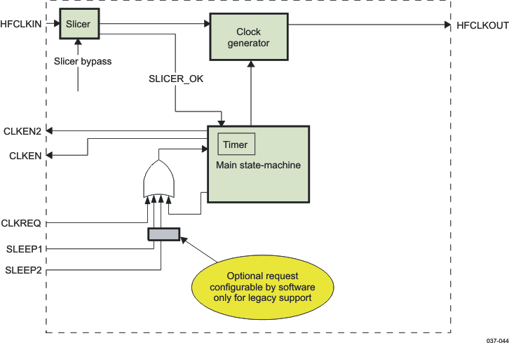 Figure 5-21 HFCLKIN Clock Distribution
When a device needs a clock signal other than 32.768 kHz, it makes a clock request and activates the CLKREQ pin. As a result, the TPS65920/TPS65930 device immediately sets CLKEN to 1 to warn the clock provider in the system about the clock request and starts a timer (maximum of 5.2 ms using the 32.768-kHz clock). When the timer expires, the TPS65920/TPS65930 device opens a gated clock, the timer automatically reloads the defined value, and a high-frequency output clock signal is available through the HFCLKOUT pin. The output drive of HFCLKOUT is programmable (minimum load 10 pF, maximum load 40 pF) and must be at 40 pF by default.
With a register setting, the mirroring of CLKEN can be enabled on CLKEN2. When this mirroring feature is not enabled, CLKEN2 can be used as a general-purpose output controlled through I2C accesses.
CLKREQ, when enabled, has a weak pulldown resistor to support the wired-OR clock request.
Figure 5-22 shows an example of the wired-OR clock request.
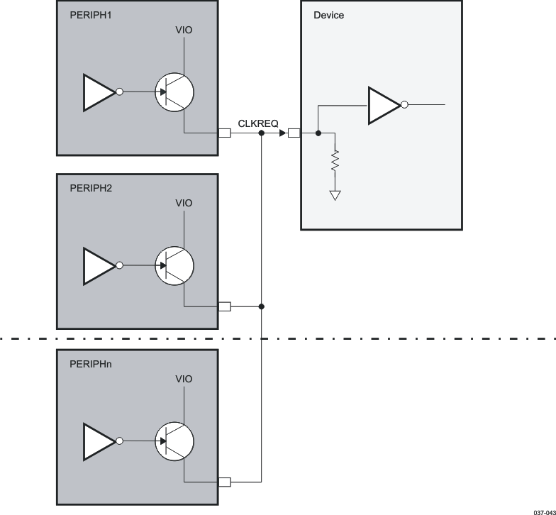 Figure 5-22 Example of Wired-OR Clock Request
The timer default value must be the worst case (10 ms) for the clock providers. For legacy or workaround support, the NSLEEP1 and NSLEEP2 signals can also be used as a clock request even if it is not their primary goal. By default, this feature is disabled and must be enabled individually by setting the register bits associated with each signal.
When the external clock signal is present on the HFCLKIN ball, it is possible to use this clock instead of the internal RC oscillator and then synchronize the system on the same clock. The RC oscillator can then go to idle mode.
Table 5-36 lists the input clock electrical characteristics of the HFCLKIN input clock.
Table 5-36 HFCLKIN Input Clock Electrical Characteristics
| PARAMETER DESCRIPTION | CONFIGURATION MODE SLICER | MIN | TYP | MAX | UNIT | |
|---|---|---|---|---|---|---|
| Frequency | 19.2, 26, or 38.4 | MHz | ||||
| Start-up time | LP(1)/HP(2) (sine wave) | 4 | μs | |||
| Input dynamic range | LP/HP (sine wave) | 0.3 | 0.7 | 1.45 | VPP | |
| BP(3)/PD(4) (square wave) | 0 | 1.85(5) | ||||
| Current consumption | LP | 175 | μA | |||
| HP | 235 | |||||
| BP/PD | 39 | nA | ||||
| Harmonic content of input signal (with 0.7-VPP amplitude): second component | LP/HP (sine wave) | –25 | dBc | |||
| VIH | Voltage input high | BP (square wave) | 1 | V | ||
| VIL | Voltage input low | BP (square wave) | 0.6 | V | ||
Table 5-37 lists the input clock timing requirements of the HFCLKIN input clock when the source is a square wave. Figure 5-23 shows the HFCLKIN squared input clock timings.
Table 5-37 HFCLKIN Square Input Clock Timing Requirements with Slicer in Bypass
| NAME | PARAMETER | DESCRIPTION | MIN | TYP | MAX | UNIT |
|---|---|---|---|---|---|---|
| CH0 | 1/tC(HFCLKIN) | Frequency, HFCLKIN | 19.2, 26, or 38.4 | MHz | ||
| CH1 | tW(HFCLKIN) | Pulse duration, HFCLKIN low or high | 0.45*tC(HFCLKIN) | 0.55*tC(HFCLKIN) | ns | |
| CH3 | tR(HFCLKIN) | Rise time, HFCLKIN(1) | 5 | ns | ||
| CH4 | tF(HFCLKIN) | Fall time, HFCLKIN(1) | 5 | ns | ||
 Figure 5-23 HFCLKIN Squared Input Clock
5.7.2.3 32-kHz Input Clock
A 32.768-kHz input clock (often abbreviated to 32-kHz) generates the clocks for the RTC. It has a low-jitter mode where the current consumption increases for lower jitter. It is possible to use the 32-kHz input clock with an external crystal or clock source. Depending on the mode chosen, the 32K oscillator is configured one of two ways:
- An external 32.768-kHz crystal through the 32KXIN/32KXOUT balls (see Figure 5-24). This configuration is available only for master mode (for more information, see Section 4.7).
- An external square/sine wave of 32.768 kHz through 32KXIN with amplitude equal to 1.8 or 1.85 V (see Figure 5-26, Figure 5-27, and Figure 5-28). This configuration is available for the master and slave modes (for more information, see Section 4.7).
5.7.2.3.1 External Crystal Description
Figure 5-24 shows the 32-kHz oscillator block diagram with crystal in master mode.
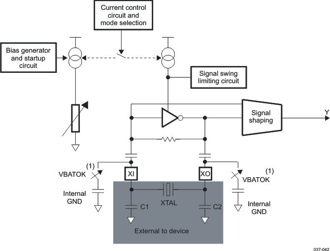
NOTE:
Switches close by default and open only if register access enables very-low-power mode when VBAT < 2.7 V.CXIN and CXOUT represent the total capacitance of the printed circuit board (PCB) and components, excluding the crystal. Their values depend on the datasheet of the crystal, the internal capacitors, and the parallel capacitor. The frequency of the oscillations depends on the value of the capacitors. The crystal must be in the fundamental mode of operation and parallel resonant.
NOTE
For the values of CXIN and CXOUT, see Table 5-48.
Table 5-38 lists the required electrical constraints.
Table 5-38 Crystal Electrical Characteristics
| PARAMETER | MIN | TYP | MAX | UNIT |
|---|---|---|---|---|
| Parallel resonance crystal frequency | 32.768 | kHz | ||
| Input voltage, Vin (normal mode) | 1.0 | 1.3 | 1.55 | V |
| Internal capacitor on each input (Cint) | 10 | pF | ||
| Parallel input capacitance (Cpin) | 1 | pF | ||
| Nominal load cap on each oscillator input CXIN and CXOUT(1) | CXIN = CXOUT = Cosc*2 – (Cint + Cpin) | pF | ||
| Pin-to-pin capacitance | 1.6 | 1.8 | pF | |
| Crystal ESR(2) | 75 | kΩ | ||
| Crystal shunt capacitance, CO | 1 | pF | ||
| Crystal tolerance at room temperature, 25°C | –30 | 30 | ppm | |
| Crystal tolerance versus temperature range (–40°C to 85°C) | –200 | 200 | ppm | |
| Maximum drive power | 1 | μW | ||
| Operating drive level | 0.5 | μW | ||
Measured with the load capacitance specified by the crystal manufacturer. If CXIN = CXOUT = 10 pF, CL = 5 pF. Parasitic capacitance from the package and board must also be considered.
When selecting a crystal, the system design must consider the temperature and aging characteristics of a crystal versus the user environment and expected lifetime of the system.
Table 5-39 and Table 5-40 list the switching characteristics of the oscillator and the timing requirements of the 32.768-kHz input clock. Figure 5-25 shows the crystal oscillator output in normal mode.
Table 5-39 Base Oscillator Switching Characteristics
| NAME | PARAMETER DESCRIPTION | MIN | TYP | MAX | UNIT | |
|---|---|---|---|---|---|---|
| fP | Oscillation frequency | 32.768 | kHz | |||
| tSX | Start-up time | 0.5 | s | |||
| IDDA | Active current consumption | LOJIT <1:0> = 00 | 1.8 | μA | ||
| LOJIT <1:0> = 11 | 8 | |||||
| IDDQ | Current consumption | Low battery mode (1.2 V) | 1 | μA | ||
| Startup | 8 | |||||
Table 5-40 32-kHz Crystal Input Clock Timing Requirements
| NAME | PARAMETER DESCRIPTION | MIN | TYP | MAX | UNIT | |
|---|---|---|---|---|---|---|
| OC0 | 1/tC(32KHZ) | Frequency, 32 kHz | 32.768 | kHz | ||
| OC1 | tW(32KHZ) | Pulse duration, 32 kHz low or high | 0.40*tC(32KHZ) | 0.60*tC(32KHZ) | μs | |
 Figure 5-25 32-kHz Crystal Input
5.7.2.3.2 External Clock Description
When an external 32K clock is used instead of a crystal, three configuration can be used:
- A square- or sine-wave input can be applied to the 32KXIN pin with amplitude of 1.85 or 1.8 V. The 32KXOUT pin can be driven to a dc value of the square- or sine-wave amplitude divided by 2. This configuration, shown in Figure 5-26, is recommended if a large load is applied on the 32KXOUT pin.
- A square- or sine-wave input can be applied to the 32KXIN pin with amplitude of 1.85 or 1.8 V. The 32KXOUT pin can be left floating. This configuration, showed in Figure 5-27, is used if no charge is applied on the 32KXOUT pin.
- The oscillator is in bypass mode and a square-wave input can be applied to the 32KXIN pin with amplitude of 1.8 V. The 32KXOUT pin can be left floating. This configuration, shown in Figure 5-28, is used if the oscillator is in bypass mode.
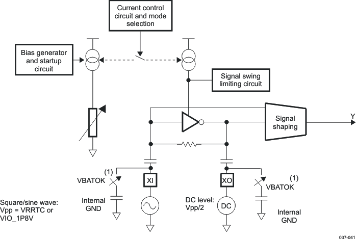
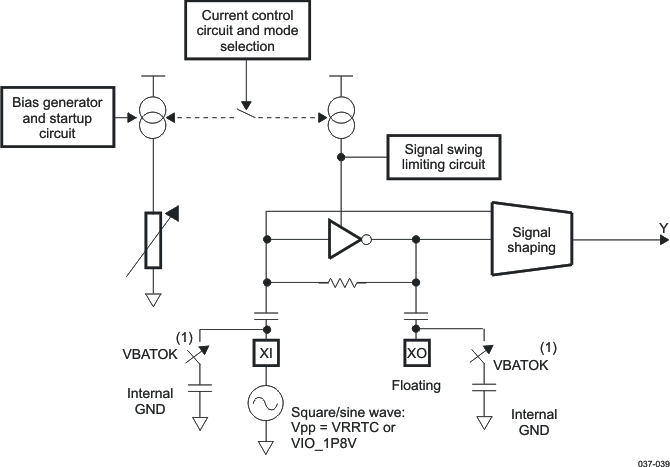
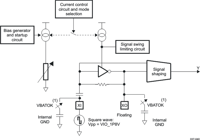
Table 5-41 lists the electrical constraints required by the 32-kHz input square- or sine-wave clock.
Table 5-41 32-kHz Input Square- or Sine-Wave Clock Source Electrical Characteristics
| NAME | PARAMETER DESCRIPTION | MIN | TYP | MAX | UNIT |
|---|---|---|---|---|---|
| f | Frequency | 32.768 | kHz | ||
| CI | Input capacitance | 35 | pF | ||
| CFI | On-chip foot capacitance to GND on each input (see Figure 5-26, Figure 5-27, and Figure 5-28) | 10 | pF | ||
| VPP | Square-/sine-wave amplitude in bypass mode or not | 1.8(1) | V | ||
| VIH | Voltage input high, square wave in bypass mode | 0.8 | V | ||
| VIL | Voltage input low, square wave in bypass mode | 0.6 | V | ||
Table 5-42 lists the timing requirements of the 32-kHz square-wave input clock.
Table 5-42 32-kHz Square-Wave Input Clock Source Timing Requirements
| NAME | PARAMETER | DESCRIPTION | MIN | TYP | MAX | UNIT |
|---|---|---|---|---|---|---|
| CK0 | 1/tC(32KHZ) | Frequency, 32 kHz | 32.768 | MHz | ||
| CK1 | tW(32KHZ) | Pulse duration, 32 kHz low or high | 0.45*tC(32KHZ) | 0.55*tC(32KHZ) | μs | |
| CK3 | tR(32KHZ) | Rise time, 32 kHz(1) | 0.1*tC(32KHZ) | μs | ||
| CK4 | tF(32KHZ) | Fall time, 32 kHz(1) | 0.1*tC(32KHZ) | μs | ||
Figure 5-29 shows the 32-kHz square- or sine-wave input clock.
 Figure 5-29 32-kHz Square- or Sine-Wave Input Clock
5.7.3 Output Clock Specifications
The TPS65920/TPS65930 device provides two output clocks:
- 32KCLKOUT
- HFCLKOUT
5.7.3.1 32KCLKOUT Output Clock
Figure 5-30 is the block diagram for the 32.768-kHz clock output.
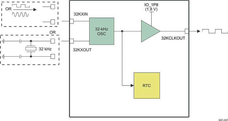 Figure 5-30 32.768-kHz Clock Output Block Diagram
The TPS65920/TPS65930 device has an internal 32.768-kHz oscillator connected to an external 32.768-kHz crystal through the 32KXIN/32KXOUT balls or an external digital 32.768-kHz clock through the 32KXIN input (see Figure 5-30). The TPS65920/TPS65930 device also generates a 32.768-kHz digital clock through the 32KCLKOUT pin and can broadcast it externally to the application processor or any other devices. The 32KCLKOUT clock is broadcast by default in TPS65920/TPS65930 active mode, but can be disabled if it is not used.
The 32.768-kHz clock (or signal) is also used to clock the RTC embedded in the TPS65920/TPS65930 device. The RTC is not enabled by default. The host processor must set the correct date and time and enable the RTC functionality.
The 32KCLKOUT output buffer can drive several devices (up to 40-pF load). At startup, 32KCLKOUT must be stabilized (frequency/duty cycle) before the signal output. Depending on the startup conditions, this can delay the startup sequence.
Table 5-43 lists the electrical characteristics of the 32KCLKOUT output clock.
Table 5-43 32KCLKOUT Output Clock Electrical Characteristics
| NAME | PARAMETER DESCRIPTION | MIN | TYP | MAX | UNIT |
|---|---|---|---|---|---|
| f | Frequency | 32.768 | kHz | ||
| CL | Load capacitance | 40 | pF | ||
| VOUT | Output clock voltage, depending on output reference level IO_1P8 (see Section 3) | 1.8(1) | V | ||
| VOH | Voltage output high | VOUT – 0.45 | VOUT | V | |
| VOL | Voltage output low | 0 | 0.45 | V |
Table 5-44 lists the output clock switching characteristics. Figure 5-31 shows the 32KCLKOUT output clock waveform.
Table 5-44 32KCLKOUT Output Clock Switching Characteristics
| NAME | PARAMETER | DESCRIPTION | MIN | TYP | MAX | UNIT |
|---|---|---|---|---|---|---|
| CK0 | 1/tC(32KCLKOUT) | Frequency | 32.768 | MHz | ||
| CK1 | tW(32KCLKOUT) | Pulse duration, 32KCLKOUT low or high | 0.40*tC(32KCLKOUT) | 0.60*tC(32KCLKOUT) | ns | |
| CK2 | tR(32KCLKOUT) | Rise time, 32KCLKOUT(1) | 16 | ns | ||
| CK3 | tF(32KCLKOUT) | Fall time, 32KCLKOUT(1) | 16 | ns |
 Figure 5-31 32KCLKOUT Output Clock
5.7.3.2 HFCLKOUT Output Clock
Table 5-45 lists the electrical characteristics of the HFCLKOUT output clock.
Table 5-45 HFCLKOUT Output Clock Electrical Characteristics
| NAME | PARAMETER DESCRIPTION | MIN | TYP | MAX | UNIT |
|---|---|---|---|---|---|
| f | Frequency | 19.2, 26, or 38.4 | MHz | ||
| CL | Load capacitance | 30 | pF | ||
| VOUT | Output clock voltage, depending on output reference level IO_1P8 (see Section 3) | 1.8(1) | V | ||
| VOH | Voltage output high | VOUT – 0.45 | VOUT | V | |
| VOL | Voltage output low | 0 | 0.45 | V | |
Table 5-46 lists the switching characteristics of the HFCLKOUT output clock.
Table 5-46 HFCLKOUT Output Clock Switching Characteristics
| NAME | PARAMETER | DESCRIPTION | MIN | TYP | MAX | UNIT |
|---|---|---|---|---|---|---|
| CHO1 | 1/tC(HFCLKOUT) | Frequency | 19.2, 26, or 38.4 | MHz | ||
| CHO2 | tW(HFCLKOUT) | Pulse duration, HFCLKOUT low or high | 0.40*tC(HFCLKOUT) | 0.60*tC(HFCLKOUT) | ns | |
| CHO3 | tR(HFCLKOUT) | Rise time, HFCLKOUT(1) | 2.6 | ns | ||
| CHO4 | tF(HFCLKOUT) | Fall time, HFCLKOUT(1) | 2.6 | ns | ||
Figure 5-32 shows the HFCLKOUT output clock waveform.
 Figure 5-32 HFCLKOUT Output Clock
5.7.3.3 Output Clock Stabilization Time
Figure 5-33 shows the 32KCLKOUT and HFCLKOUT clock stabilization time.
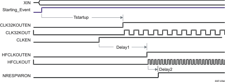
NOTE:
Tstartup, Delay1, and Delay2 depend on the boot mode (see Section 5.1.5).NOTE:
Ensure that the high frequency oscillator start-up time is in spec for the boot mode used. During power-up the internal delay, Delay1 above is fixed (5.2 ms and 5.3 ms depending on boot mode). The start-up time for the oscillator must be less than the fixed delay.Figure 5-34 shows the HFCLKOUT behavior.
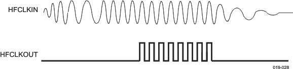 Figure 5-34 HFCLKOUT Behavior
5.8 Debouncing Time
Table 5-47 lists the characteristics of debouncing.
Table 5-47 Debouncing
| DEBOUNCING FUNCTIONS | BLOCK | PROGRAMMABLE | DEBOUNCING TIME | DEFAULT |
|---|---|---|---|---|
| USB plug detection | USB | No | 9x50 ms | 9x50 ms |
| Plug/unplug detection VBUS(1) | USB | Yes | 0 to 250 ms (32/32468-second steps) |
28 ms |
| Plug/unplug detection ID(2) | USB | Yes | 0 to 250 ms (32/32468-second steps) |
50 ms |
| Debouncing function interrupt generation debounce for VBUS and ID(3) | Power | Yes | 0 to 250 ms | 30 ms |
| Hot-die detection | Thermistor | No | 60 μs | 60 μs |
| Thermal shutdown detection | No | 60 μs | 60 μs | |
| PWRON(4) | Start/stop button | No | 31.25 ms | 31.25 ms |
| NRESWARM | Button reset | No | 60 μs | 60 μs |
| SIM card plug/unplug | GPIO | Yes | 0 or 30 ms ± 1 ms | 0 ms |
| MMC1 (plug/unplug) | GPIO | Yes | 0 or 30 ms ± 1 ms | 0 ms |
Figure 5-35 is a sample debouncing sequence chronogram.
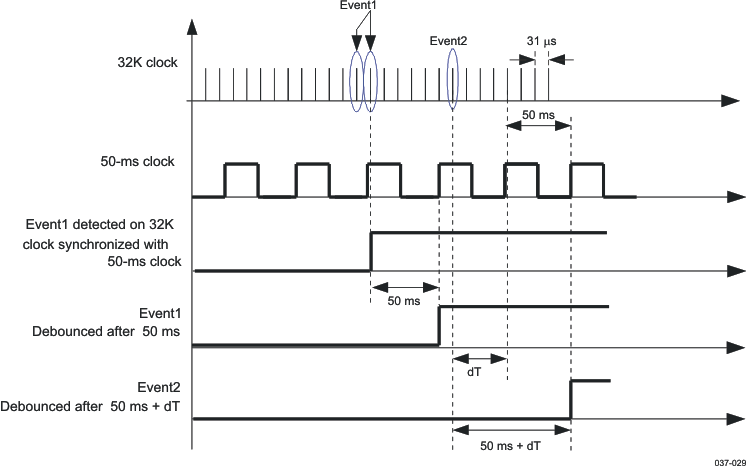 Figure 5-35 Debouncing Sequence Chronogram Example
Event1 is correctly debounced after 5 ms. Event2 is debounced after 50ms + dT because the capture of the event is considered after the next rising edge of the 50-ms clock.
5.9 External Components
Table 5-48 lists the TPS65920/TPS65930 device external components.
Table 5-48 TPS65920/TPS65930 External Components
| FUNCTION | COMPONENT | REFERENCE | VALUE | NOTE | LINK |
|---|---|---|---|---|---|
| Power Supplies | |||||
| VDD1 | Capacitor | CVDD1.IN | 10 μF | Range ± 50% ESR min = 1 mΩ ESR max = 20 mΩ Taiyo Yuden: JMK212BJ106KD |
Figure 5-1 |
| Capacitor | CVDD1.OUT | 10 μF | Range ± 50% ESR min = 1 mΩ ESR max = 20 mΩ Taiyo Yuden: JMK212BJ106KD |
||
| Inductor | LVDD1 | 1 μH | Range ± 30% DCR max = 100 mΩ |
||
| VDD2 | Capacitor | CVDD2.IN | 10 μF | Range ± 50% ESR min = 1 mΩ ESR max = 20 mΩ Taiyo Yuden: JMK212BJ106KD |
Figure 5-1 |
| Capacitor | CVDD2.OUT | 10 μF | Range ± 50% ESR min = 1 mΩ ESR max = 20 mΩ Taiyo Yuden: JMK212BJ106KD |
||
| Inductor | LVDD2 | 1 μH | Range ± 30% DCR max = 100 mΩ |
||
| VIO | Capacitor | CVIO.IN | 10 μF | Range ± 50% ESR min = 1 mΩ ESR max = 20 mΩ Taiyo Yuden: JMK212BJ106KD |
Figure 5-1 |
| Capacitor | CVIO.OUT | 10 μF | Range ± 50% ESR min = 1 mΩ ESR max = 20 mΩ Taiyo Yuden: JMK212BJ106KD |
||
| Inductor | LVVIO | 1 μH | Range ± 30% DCR max = 100 mΩ |
||
| VRUSB_3V | Capacitor | CVUSB.3P1 | 1 μF | Range: 0.3 to 2.7 μF ESR min = 20 mΩ ESR max = 300 mΩ |
Figure 5-1Figure 5-13 |
| VRUSB_1V5 | Capacitor | CVINTUSB1P5.OUT | 1 μF | Range: 0.3 to 2.7 μF ESR min = 20 mΩ ESR max = 600 mΩ |
Figure 5-1Figure 5-13 |
| VRUSB_1V8 | Capacitor | CVINTUSB1P8.OUT | 1 μF | Range: 0.3 to 2.7 μF ESR min = 20 mΩ ESR max = 600 mΩ |
Figure 5-1Figure 5-13 |
| VDAC | Capacitor | CVDAC.IN | 1 μF | Range: 0.3 to 2.7 μF ESR min = 20 mΩ ESR max = 600 mΩ |
Figure 5-1 |
| Capacitor | CVDAC.OUT | 1 μF | Range: 0.3 to 2.7 μF ESR min = 20 mΩ ESR max = 600 mΩ |
||
| VPLLA3R | Capacitor | CVPLLA3R.IN | 1 μF | Range: 0.3 to 2.7 μF ESR min = 20 mΩ ESR max = 600 mΩ |
Figure 5-1 |
| VPLL1 | Capacitor | CVPLL1.OUT | 1 μF | Range: 0.3 to 2.7 μF ESR min = 20 mΩ ESR max = 600 mΩ |
Figure 5-1 |
| VMMC1 | Capacitor | CVMMC1.IN | 1 μF | Range: 0.3 to 2.7 μF ESR min = 20 mΩ ESR max = 600 mΩ |
Figure 5-1 |
| Capacitor | CVMMC1.OUT | 1 μF | Range: 0.3 to 2.7 μF ESR min = 20 mΩ ESR max = 600 mΩ |
||
| VAUX12S | Capacitor | CVAUX12S.IN | 1 μF | Range: 0.3 to 2.7 μF ESR min = 20 mΩ ESR max = 600 mΩ |
Figure 5-1 |
| VAUX2 | Capacitor | CVAUX2.OUT | 1 μF | Range: 0.3 to 2.7 μF ESR min = 20 mΩ ESR max = 600 mΩ |
Figure 5-1 |
| VINT | Capacitor | CVINT.IN | 1 μF | Range: 0.3 to 2.7 μF ESR min = 20 mΩ ESR max = 600 mΩ |
Figure 5-1 |
| VINTANA1 | Capacitor | CVINTANA1.OUT | 1 μF | Range: 0.3 to 2.7 μF ESR min = 20 mΩ ESR max = 600 mΩ |
Figure 5-1 |
| VINTANA2 | Capacitor | CVINTANA2.OUT | 1 μF | Range: 0.3 to 2.7 μF ESR min = 20 mΩ ESR max = 600 mΩ |
Figure 5-1 |
| VINTDIG | Capacitor | CVINTDIG.OUT | 1 μF | Range: 0.3 to 2.7 μF ESR min = 20 mΩ ESR max = 600 mΩ |
Figure 5-1 |
| VBAT.USB | Capacitor | CVBAT.USB | 1 μF | Range: 0.3 to 2.7 μF ESR min = 20 mΩ ESR max = 600 mΩ |
Figure 5-13 |
| USB CP | Capacitor | CVBUS.FC | 2.2 μF ± 40% | ESR max = 20 mΩ | Figure 5-13 |
| Capacitor | CVBUS.IN | 10 μF | |||
| Capacitor | CVBUS | 4.7 μF ± 40% | ESR max = 20 mΩ | ||
| 32.768 kHz | |||||
| 32K OSC | Capacitor | CXIN | 10 pF | Range: 9 pF to 12.5 pF | Figure 5-24 |
| Capacitor | CXOUT | 10 pF | |||
| Quartz | X32.768kHz | 32.768 kHz | ±30 ppm (at 25°C) ±200 ppm (–40°C to 85°C) |
||
| Audio | |||||
| External class-D predriver left | Capacitor | CPL.O | 50 pF | Figure 6-2 | |
| Capacitor | CPL | 1 μF | |||
| Resistor | RPL | >15 kΩ | |||
| Resistor | RPL.M | >15 kΩ | |||
| Resistor | RPL.O | 10 kΩ | |||
| Capacitor | CPL.M | 1 μF | |||
| External class-D predriver right | Capacitor | CPR.O | 50 pF | Figure 6-2 | |
| Capacitor | CPR | 1 μF | |||
| Resistor | RPR | >15 kΩ | |||
| Resistor | RPR.M | >15 kΩ | |||
| Resistor | RPR.O | 10 kΩ | |||
| Capacitor | CPR.M | 1 μF | |||
| Vibrator H-bridge | Ferrite bead | LV.M | BLM18BD221S1N | Figure 6-3 | |
| Ferrite bead | LV.P | BLM18BD221S1N | |||
| Capacitor | CV.V | 1 μF | |||
| Capacitor | CV.M | 1 nF | |||
| Capacitor | CV.P | 1 nF | |||
| MIC main (pseudo differential mode) | Capacitor | CMM.M | 100 nF | Figure 6-6 | |
| Capacitor | CMM.P | 100 nF | |||
| Capacitor | CMM.O | 47 pF | |||
| Resistor | RMM.O | ~500 Ω | |||
| Resistor | RMM.MP | ~1.7 kΩ | |||
| Capacitor | CMM.B | 0 to 200 pF | If greater than 200 pF, a serial resistor is required for bias stability | ||
| MIC main (differential mode) | Capacitor | CMM.M | 100 nF | Figure 6-7 | |
| Capacitor | CMM.P | 100 nF | |||
| Capacitor | CMM.PM | 47 pF | |||
| Capacitor | CMM.O | 47 pF | |||
| Capacitor | CMM.GM | 47 pF | |||
| Capacitor | CMM.GP | 47 pF | |||
| Resistor | RMM.BP | 1 kΩ | |||
| Resistor | RMM.GM | 1 kΩ | |||
| Capacitor | CMM.B | 0 to 200 pF | If greater than 200 pF, a serial resistor is required for bias stability | ||
| VMIC1 | Capacitor | CVMIC1.OUT | 1 μF | Range: 0.3 μF to 3.3 μF ESR min = 20 mΩ ESR max = 600 mΩ |
|
| Silicon MIC | Capacitor | CSM | 1 μF | Figure 6-8 | |
| Capacitor | CSM.P | 100 nF | |||
| Capacitor | CSM.M | 100 nF | |||
| Capacitor | CSM.PG | 47 nF | |||
| Resistor | RSM | >500 Ω | |||
| Auxiliary right | Capacitor | CAUXR | 100 nF | Figure 6-9 | |
| Capacitor | CAUXR.M | 47 pF | |||
| LED Driver | |||||
| LED | Resistor | RLED.A | 120 Ω | Needed for each LED | Figure 5-18 |
| Resistor | RLED.B | 160 kΩ | Needed for each LED | ||
| I2C Bus—External Pullup | |||||
| I2C SmartReflex | Resistor | RPSR.SDA | Pullups for various bus capacitances (CL) and I2C speeds (Std, Fast, and HS) If CL = 10 pF: Std = 118 kΩ, Fast = 35.4 kΩ, HS = 4.7 kΩ If CL = 12 pF: Std = 98.3 kΩ, Fast = 29.5 kΩ, HS = 3.9 kΩ If CL = 50 pF: Std = 23.6 kΩ, Fast = 7.1 kΩ, HS = 940 Ω If CL = 100 pF: Std = 11.8 kΩ, Fast = 3.54 kΩ, HS = 470 Ω If CL ≤ 12 pF, there is no need for an external pullup, the internal 3-kΩ pullup can be used. If an external pullup is used, disable the internal 3-kΩ pullup (reference the GPPUPDCTR1 register; see the TRM). |
Section 4.7.3 | |
| Resistor | RPSR.SCL | ||||
| I2C control | Resistor | RCNTL.SD; | |||
| Resistor | RCNTL.SCL | ||||