SGLS303F May 2005 – April 2016 TPS732-Q1
PRODUCTION DATA.
- 1 Features
- 2 Applications
- 3 Description
- 4 Revision History
- 5 Pin Configuration and Functions
- 6 Specifications
- 7 Detailed Description
- 8 Application and Implementation
- 9 Power Supply Recommendations
- 10Layout
- 11Device and Documentation Support
- 12Mechanical, Packaging, and Orderable Information
Package Options
Mechanical Data (Package|Pins)
Thermal pad, mechanical data (Package|Pins)
- DRB|8
Orderable Information
1 Features
- Qualified for Automotive Applications
- AEC-Q100 Qualified With the Following Results
- Device Temperature Grade 0: –40°C to 150°C Ambient Operating Temperature Range
- Device HBM Classification Level 2
- Device CDM Classification Level C4B
- Device MM Classification Level M2
- Stable With No Output Capacitor or Any Value or Type of Capacitor
- Input Voltage Range: 1.7 V to 5.5 V
- Ultra-Low Dropout Voltage: 40-mV Typical at 250 mA
- Excellent Load Transient Response—With or Without Optional Output Capacitor
- New NMOS Topology Provides Low Reverse Leakage Current
- Low Noise: 30-μVRMS Typical (10 kHz to 100 kHz)
- 0.5% Initial Accuracy
- 1% Overall Accuracy (Line, Load, and Temperature)
- Less Than 1-μA Maximum IQ in Shutdown Mode
- Thermal Shutdown and Specified Minimum and Maximum Current Limit Protection
- Available in Multiple Output Voltage Versions
- Fixed Outputs of 1.2 V, 1.5 V, 1.6 V, 1.8 V,
2.5 V, 3 V, 3.3 V, and 5 V - Adjustable Outputs From 1.2 V to 5.5 V
- Custom Outputs Available
- Fixed Outputs of 1.2 V, 1.5 V, 1.6 V, 1.8 V,
2 Applications
- Portable and Battery-Powered Equipment
- Post-Regulation for Switching Supplies
- Noise-Sensitive Circuitry Such as VCOs
- Point of Load Regulation for DSPs, FPGAs, ASICs, and Microprocessors
3 Description
The TPS732-Q1 family of low-dropout (LDO) voltage regulators uses a new topology: an NMOS pass element in a voltage-follower configuration. This topology is stable using output capacitors with low ESR, and even allows operation without a capacitor. The topology also provides high reverse blockage (low reverse current) and ground pin current that is nearly constant over all values of output current.
The TPS732-Q1 family of devices uses an advanced BiCMOS process to yield high precision while delivering low dropout voltages and low ground pin current. Current consumption, when not enabled, is under 1 μA and ideal for portable applications. The extremely low output noise (30 μVRMS with 0.1-µF CNR) is ideal for powering VCOs. These devices are protected by thermal shutdown and foldback current limit.
Device Information(1)
| PART NUMBER | PACKAGE | BODY SIZE (NOM) |
|---|---|---|
| TPS73201-Q1 | SOT-23 (5) | 2.90 mm × 1.60 mm |
| VSON (8) | 3.00 mm × 3.00 mm |
- For all available packages, see the orderable addendum at the end of the datasheet.
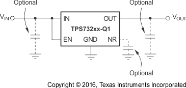
Typical Application Circuit for Fixed Voltage Versions
