SGLS118D December 2001 – September 2016
PRODUCTION DATA.
- 1 Features
- 2 Applications
- 3 Description
- 4 Revision History
- 5 Description (continued)
- 6 Pin Configuration and Functions
- 7 Specifications
- 8 Detailed Description
- 9 Application and Implementation
- 10Power Supply Recommendations
- 11Layout
- 12Device and Documentation Support
- 13Mechanical, Packaging, and Orderable Information
Package Options
Refer to the PDF data sheet for device specific package drawings
Mechanical Data (Package|Pins)
- DBV|5
Thermal pad, mechanical data (Package|Pins)
Orderable Information
1 Features
- Qualified for Automotive Applications
- 100-mA Low-Dropout Regulator
- Available in 1.2-V, 1.5-V, 1.8-V, 2.5-V, 2.7-V, 2.8‑V, 3-V, 3.3-V and 5-V Fixed-Output and Adjustable Versions
- Only 17-µA Quiescent Current at 100 mA
- 1-µA Quiescent Current in Standby Mode
- Dropout Voltage Typically 71 mV at 100 mA
- Overcurrent Limitation
- —40°C to 125°C Operating Junction Temperature Range
- 5-Pin SOT-23 (DBV) Package
2 Applications
- ADAS Modules
- RF Modules
- Wireless Modules
- General Noise-Sensitive Applications
3 Description
The TPS769xx-Q1 family of low-dropout (LDO) voltage regulators offers the benefits of low-dropout voltage, ultralow-power operation, and miniaturized packaging. These regulators feature low-dropout voltages and ultralow quiescent current compared to conventional LDO regulators. Offered in a 5-pin small outline integrated-circuit SOT-23 package, the TPS769xx-Q1 series of devices are ideal for micropower operations and where board space is at a premium.
A combination of new circuit design and process innovation has enabled the usual PNP pass transistor to be replaced by a PMOS pass element. Because the PMOS pass element behaves as a low-value resistor, the dropout voltage is very low, typically 71 mV at 100 mA of load current (TPS76950-Q1), and is directly proportional to the load current. Because the PMOS pass element is a voltage-driven device, the quiescent current is ultralow (28 µA maximum) and is stable over the entire range of output load current (0 mA to 100 mA). The ultralow-dropout voltage feature and ultralow-power operation result in a significant increase in system battery operating life, making this device suitable for use in automotive applications.
Device Information(1)
| PART NUMBER | PACKAGE | BODY SIZE (NOM) |
|---|---|---|
| TPS769xx-Q1 | SOT-23 (5) | 2.90 mm × 1.60 mm |
- For all available packages, see the orderable addendum at the end of the data sheet.
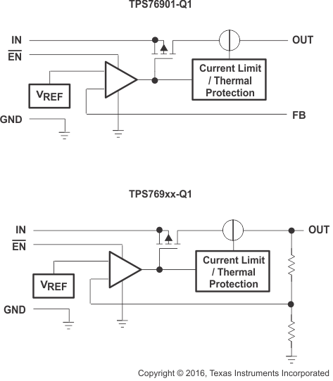
Functional Block Diagrams

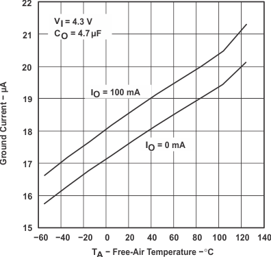
TPS76933-Q1 Ground Current vs Free-Air Temperature
