SBVS263A July 2017 – September 2017 TPS7A39
PRODUCTION DATA.
- 1 Features
- 2 Applications
- 3 Description
- 4 Revision History
- 5 Pin Configuration and Functions
- 6 Specifications
- 7 Detailed Description
-
8 Application and Implementation
- 8.1
Application Information
- 8.1.1 Setting the Output Voltages on Adjustable Devices
- 8.1.2 Capacitor Recommendations
- 8.1.3 Input and Output Capacitor (CINx and COUTx)
- 8.1.4 Feed-Forward Capacitor (CFFx)
- 8.1.5 Noise-Reduction and Soft-Start Capacitor (CNR/SS)
- 8.1.6 Buffered Reference Voltage
- 8.1.7 Overriding Internal Reference
- 8.1.8 Start-Up
- 8.1.9 AC and Transient Performance
- 8.1.10 DC Performance
- 8.1.11 Reverse Current
- 8.1.12 Power Dissipation (PD)
- 8.2 Typical Applications
- 8.1
Application Information
- 9 Power-Supply Recommendations
- 10Layout
- 11Device and Documentation Support
- 12Mechanical, Packaging, and Orderable Information
Package Options
Mechanical Data (Package|Pins)
- DSC|10
Thermal pad, mechanical data (Package|Pins)
- DSC|10
Orderable Information
7 Detailed Description
7.1 Overview
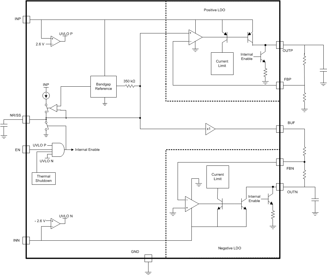
The TPS7A39 is an innovative linear regulator (LDO) targeted at powering the signal chain, capable of up to ±33 V on the inputs and regulating up to ±30 V on the outputs at up to 150 mA of load current. The device uses an LDO topology that, by design, delivers ratiometric start-up tracking in most applications. The TPS7A39 has several other features, as listed in Table 1, that simplify using the device in a variety of applications.
NOTE
Throughout this document, x is used to designate that the condition or component applies to both the positive and negative regulators (for example, CFFx means CFFP and CFFN).
Table 1. TPS7A39 Features
| VOLTAGE REGULATION | SYSTEM START-UP | INTERNAL PROTECTION |
|---|---|---|
| Reference input/output | Ratiometric start-up tracking | Current limit |
| High-PSRR output | Programmable soft-start | Thermal shutdown |
| Fast transient response | Sequencing controls |
7.2 Functional Block Diagram
7.3 Feature Description
7.3.1 Voltage Regulation
7.3.1.1 DC Regulation
An LDO functions as a buffered op-amp in which the input signal is the internal reference voltage (VNR/SS), as shown in Figure 59, and in normal regulation VFBP = VNR/SS. Sharing a single reference ensures that both channels track each other during start-up.
VNR/SS is designed to have a very low-bandwidth at the input to the error amplifier through the use of a low-pass filter. As such, the reference can be considered as a pure dc input signal.
As Figure 60 shows, the negative LDO on the device regulates with a VFBN = 0 V and inverts the positive reference (VBUF). This topology allows the negative regulator to regulate down to 0 V.
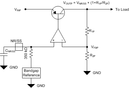 Figure 59. Simplified Positive Regulation Circuit
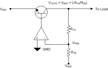 Figure 60. Simplified Negative Regulation Circuit
7.3.1.2 AC and Transient Response
Each LDO responds quickly to a transient on the input supply (line transient) or the output current (load transient). This LDO has a high power-supply rejection ratio (PSRR) and, when coupled with a low internal noise-floor (Vn), the LDO approximates an ideal power supply in ac and large-signal conditions.
The performance and internal layout of the device minimizes the coupling of noise from one channel to the other channel (crosstalk). Good printed circuit board (PCB) layout minimizes the crosstalk.
The noise-reduction and soft-start capacitor (CNR/SS) and feed-forward capacitor (CFFx) easily reduce the device noise floor and improve PSRR; see the Optimizing Noise and PSRR section for more information on optimizing the noise and PSRR performance.
7.3.2 User-Settable Buffered Reference
As Figure 61 shows, the device internally generated band-gap voltage outputs at the NR/SS pin. An internal resistor (RNR) and an external capacitor (CNR/SS) control the rise time of the voltage at the VNR/SS pin, setting the soft-start time. This network also filters out noise from the band gap, reducing the overall noise floor of the device.
Driving the NR/SS pin with an external source can improve the device accuracy and can reduce the device noise floor, along with enabling the device to regulate the positive channel to voltages below the device internal reference.
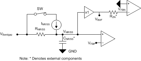
NOTE:
* denotes external components.7.3.3 Active Discharge
When either EN or UVLOx are low, the device connects a resistance from VOUTx to GND, discharging the output capacitance. The active discharge circuit requires |VOUTx| ≥ 0.6 V (typ) to discharge the output because the NPN pulldown has a minimum VCE requirement.
Do not rely on the active discharge circuit for discharging large output capacitors when the input voltage drops below the targeted output voltage. The TPS7A39 is a bipolar device, and as such, reverse voltage conditions (|VOUTx| ≥ |VINX| + 0.3 V) can breakdown the emitter to base diode and also cause a breakdown of the parasitic bipolar formed in the substrate; see the Reverse Current section for more details.
When either EN or UVLOx are low, the device outputs a small amount of leakage current. The leakage current is typically handled by the maximum R2x resistor value of 240 kΩ. However, if the device is placed in unity gain (no R2x resistor) this leakage current causes the output to slowly rise until the discharge circuit (as shown in Figure 62) has enough headroom to clamp the output voltage (typically ±0.6 V).
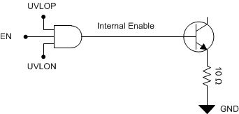 Figure 62. Simplified Active Discharge Circuit
7.3.4 System Start-Up Controls
In many different applications, the power-supply output must turn-on within a specific window of time because of sequencing requirements, ensuring proper operation of the load, or to minimize the loading on the input supply.
Both LDOs start-up are well-controlled and user-adjustable through the CNR/SS capacitor, solving the demanding requirements faced by many power-supply design engineers in a simple fashion. For start-up tracking to work correctly. a minimum 4.7-nF CNR/SS capacitor is required. For more information on startup tracking, see the Noise-Reduction and Soft-Start Capacitor (CNR/SS) section.
7.3.4.1 Start-Up Tracking
Figure 63 shows how both regulators use a common reference, which enables start-up tracking. Using the same reference voltage for both the positive and negative regulators ensures that the regulators start-up together in a controlled fashion; see Figure 24 and Figure 25.
Ramps on VINx with EN = VINP that are slower than the soft-start time do not have start-up tracking. If ramps slower than the soft-start time are used then enable should be used to start the device to ensure start-up tracking. A small mismatch between the positive and negative internal enable thresholds means that one channel turns on at a slightly lower input voltage than the other channel. This mismatch is typically not a problem in most applications and is easily solved by controlling the start-up with enable. The external signal can come from the input power supply power-good indicator, a voltage supervisor output such as the TPS3701, or from another source.
7.3.4.2 Sequencing
Figure 64 and Table 2 describe how the turn-on and turn-off times of both LDOs (respectively) is controlled by setting the enable circuit (EN) and undervoltage lockout circuit (UVLOP and UVLON).
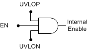 Figure 64. Simplified Turn-On Control
Table 2. Sequencing Functionality Table
| POSITIVE INPUT VOLTAGE (VINP) | NEGATIVE INPUT VOLTAGE (VINN) | ENABLE STATUS | LDO STATUS | ACTIVE DISCHARGE |
|---|---|---|---|---|
| VINP ≥ VUVLOP | VINN ≤ VUVLON | EN = 1 | On | Off |
| EN = 0 | Off | On(1) | ||
| VINP ≥ VUVLOP | VINN > VUVLON | EN = don't care | Off | On(1) |
| VINP < VUVLOP | VINN ≤ VUVLON | EN = don't care | Off | On(1) |
| VINP < VUVLOP – VHYSP | VINN > VUVLON – VHYSN | EN = don't care | Off | On(1) |
7.3.4.2.1 Enable (EN)
The enable signal (VEN) is an active-high digital control that enables the LDO when the enable voltage is past the rising threshold (VEN ≥ VIH(EN)) and disables the LDO when the enable voltage is below the falling threshold (VEN ≤ VIL(EN)). The exact enable threshold is between VIH(EN) and VIL(EN) because EN is a digital control. In applications that do not use the enable control, connect EN to VINP.
A slow VINx ramp directly connecting EN to VINP can cause the start-up tracking to move out of specification. Under slow ramp conditions, use a resistor divider from VINP to ensure start-up tracking.
7.3.4.2.2 Undervoltage Lockout (UVLO) Control
The UVLO circuit responds quickly to glitches on the input supplies and attempts to disable the output of the device if either of these rails collapse.
As a result of the fast response time of the input supply UVLO circuit, fast and short line transients well below the input supply UVLO falling threshold (brownouts) can cause momentary glitches during the edges of the transient. These glitches are typical in most LDOs. The local input capacitance prevents severe brown-outs in most applications; see the Undervoltage Lockout (UVLOx) Control section for more details. Fast line transients can cause the outputs to momentarily shut off, and can be mitigated through using the recommended 10-µF input capacitor. If this becomes a problem in the system, increasing the input capacitance prevents these glitches from occurring.
7.4 Device Functional Modes
7.4.1 Normal Operation
The device regulates to the nominal output voltage under the following conditions:
- The input voltage is at least as high as |VINx(min)|
- The input voltage is greater than the nominal output voltage added to the dropout voltage
- The enable voltage has previously exceeded the enable rising threshold voltage and has not decreased below the enable falling threshold
- The output current is less than the current limit
- The device junction temperature is less than TSD
7.4.2 Dropout Operation
If the input voltage is lower than the nominal output voltage plus the specified dropout voltage, but all other conditions are met for normal operation, the device operates in dropout mode. In this mode of operation, the output voltage is the same as the input voltage minus the dropout voltage. The transient performance of the device is significantly degraded because the pass device (as a bipolar junction transistor, or BJT) is in saturation and no longer controls the current through the LDO. Line or load transients in dropout can result in large output voltage deviations.
7.4.3 Disabled
The device is disabled under the following conditions:
- The enable voltage is less than the enable falling threshold voltage or has not yet exceeded the enable rising threshold
- The device junction temperature is greater than the thermal shutdown temperature
Table 3 shows the conditions that lead to the different modes of operation.
Table 3. Device Functional Mode Comparison
| OPERATING MODE | PARAMETER | |||
|---|---|---|---|---|
| VIN | VEN | IOUT | TJ | |
| Normal mode | |VINx| > |VOUT(nom)| + |VDOx| and |VINx| > |VINx(min)| |
VEN > VIH | |IOUTx| < |ILIMx| | T J < 125°C |
| Dropout mode | |VINx(min)| < |VINx| < |VOUTx(nom)| + |VDOx| | VEN > VIH | — | TJ < 125°C |
| Disabled mode (any true condition disables the device) |
— | VEN < VIL | — | TJ > TSD |