SLVSC31D December 2013 – August 2015 TPS7A4501-SP
PRODUCTION DATA.
- 1 Features
- 2 Applications
- 3 Description
- 4 Revision History
- 5 Description (continued)
- 6 Pin Configuration and Functions
- 7 Specifications
- 8 Detailed Description
- 9 Application and Implementation
- 10Power Supply Recommendations
- 11Layout
- 12Device and Documentation Support
- 13Mechanical, Packaging, and Orderable Information
Package Options
Mechanical Data (Package|Pins)
Thermal pad, mechanical data (Package|Pins)
Orderable Information
1 Features
- QMLV Qualified SMD 5962-12224
- Adjustable Output from 1.21 to 20 V
- Optimized for Fast-Transient Response
- High Output Voltage Accuracy: 1.15% at 25°C (Typical)
- Dropout Voltage: 200 mV With ILOAD = 750 mA (Typical)
- Low Noise: 50 μVRMS (10 Hz to 100 kHz) for VOUT = 5 V
- High Ripple Rejection: 68 dB at 1 kHz
- 1-mA Quiescent Current
- No Protection Diodes Needed
- Stable With Ceramic Output Capacitor
- Reverse-Battery Protection
- Reverse Current Protection
- 5962-1222402VHA:
- Wide Vin 2.3 to 20 V
- Output Current: 750 mA
- 5962R1222403VXC:
- Wide Vin 2.9 to 20 V
- Output Current: 1.5 A
- Thermally-Enhanced HKU Package
- Radiation Hardness Assurance (RHA) up to Total Ionizing Dose (TID) 100 krad (Si)
- Exhibits Low Dose Rate Sensitivity But Remains Within the Pre-Radiation Electrical Limits at 100 krad Total Dose Level, as Allowed by MIL-STD-883, TM1019
2 Applications
- RF Components VCOs, Receivers, ADCs, Amplifiers and Clock Distributions
- Clean Analog Supply Requirements
- Available in Military (–55°C to 125°C) Temperature Range
- Engineering Evaluation (/EM) Samples are Available (1)
(1) These units are intended for engineering evaluation only. They are processed to a non-compliant flow (for example, no burn-in, and so forth) and are tested to a temperature rating of 25°C only. These units are not suitable for qualification, production, radiation testing or flight use. Parts are not specified for performance over the full MIL specified temperature range of –55°C to 125°C or operating life.
3 Description
The TPS7A4501-SP is a low-dropout (LDO) regulator optimized for fast-transient response. The 5962-1222402VHA can supply 750 mA of output current with a dropout voltage of 300 mV. The 5962R1222403VXC can supply 1.5 A of output current with a dropout voltage of 320 mV. Quiescent current is well controlled; it does not rise in dropout, as with many other regulators. In addition to fast transient response, the TPS7A4501-SP regulator has very-low output noise, which makes it ideal for sensitive RF supply applications.
Device Information(1)
| PART NUMBER | PACKAGE | BODY SIZE (NOM) |
|---|---|---|
| TPS7A4501-SP | CFP [U] (10) | 6.35 mm × 6.35 mm |
| CFP [HKU] (10) | 7.02 mm × 6.86 mm | |
| KGD | N/A(2) |
- For all available packages, see the orderable addendum at the end of the data sheet.
- Bare die in waffle pack
SPACE
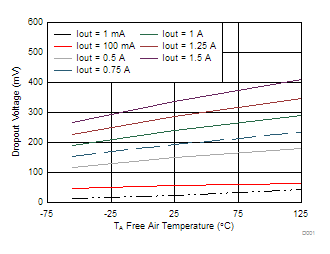
Dropout Voltage vs Temperature

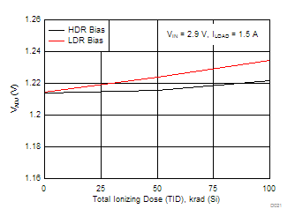
VADJ Radiation Drift Curve
