SBVS281A March 2016 – July 2016 TPS7A87
PRODUCTION DATA.
- 1 Features
- 2 Applications
- 3 Description
- 4 Revision History
- 5 Pin Configuration and Functions
- 6 Specifications
- 7 Detailed Description
- 8 Application and Implementation
- 9 Power Supply Recommendations
- 10Layout
- 11Device and Documentation Support
- 12Mechanical, Packaging, and Orderable Information
Package Options
Refer to the PDF data sheet for device specific package drawings
Mechanical Data (Package|Pins)
- RTJ|20
Thermal pad, mechanical data (Package|Pins)
- RTJ|20
Orderable Information
8 Application and Implementation
NOTE
Information in the following applications sections is not part of the TI component specification, and TI does not warrant its accuracy or completeness. TI’s customers are responsible for determining suitability of components for their purposes. Customers should validate and test their design implementation to confirm system functionality.
8.1 Application Information
Successfully implementing an LDO in an application depends on the application requirements. This section discusses key device features and how to best implement them to achieve a reliable design.
8.1.1 External Component Selection
8.1.1.1 Setting the Output Voltage (Adjustable Operation)
Each LDO resistor feedback network sets the output voltage, as shown in Figure 45, with an output voltage range of 0.8 V to 5.2 V.
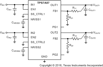 Figure 45. Adjustable Operation
Equation 1 relates the values R1x and R2x to VOUTx(Target) and VFBx. Equation 1 is a rearranged version of Equation 2, simplifying the feedback resistor calculation. The current through the feedback network must be equal to or greater than 5 μA for optimum noise performance and accuracy, as shown in Equation 3.
The input bias current into the error amplifier (feedback pin current, IFBx) and tighter tolerance resistors must be taken into account for optimizing the output voltage accuracy.
Table 4 shows the resistor combinations for several common output voltages using commercially-available, 1% tolerance resistors.
Table 4. Recommended Feedback-Resistor Values
| TARGETED OUTPUT VOLTAGE (V) | FEEDBACK RESISTOR VALUES(1) | CALCULATED OUTPUT VOLTAGE (V) | |
|---|---|---|---|
| R1x (kΩ) | R2x (kΩ) | ||
| 0.80 | Short | Open | 0.800 |
| 0.90 | 1.37 | 11.0 | 0.900 |
| 0.95 | 1.91 | 10.2 | 0.950 |
| 1.00 | 2.55 | 10.2 | 1.000 |
| 1.05 | 3.32 | 10.7 | 1.048 |
| 1.10 | 3.57 | 9.53 | 1.100 |
| 1.15 | 4.64 | 10.7 | 1.147 |
| 1.20 | 5.49 | 11.0 | 1.199 |
| 1.35 | 6.98 | 10.2 | 1.347 |
| 1.50 | 9.31 | 10.7 | 1.496 |
| 1.80 | 13.70 | 11.0 | 1.796 |
| 1.90 | 14.70 | 10.7 | 1.899 |
| 2.50 | 22.60 | 10.7 | 2.490 |
| 2.85 | 27.40 | 10.7 | 2.849 |
| 3.00 | 29.40 | 10.7 | 2.998 |
| 3.30 | 33.20 | 10.7 | 3.282 |
| 3.60 | 35.70 | 10.2 | 3.600 |
| 4.50 | 44.20 | 9.53 | 4.510 |
| 5.00 | 56.20 | 10.7 | 5.002 |
| 5.20 | 53.60 | 9.76 | 5.193 |
8.1.1.2 Capacitor Recommendations
The device is designed to be stable using low equivalent series resistance (ESR) ceramic capacitors at the input and output pins. Multilayer ceramic capacitors have become the industry standard for these types of applications and are recommended, but must be used with good judgment. Ceramic capacitors that employ X7R-, X5R-, and COG-rated dielectric materials provide relatively good capacitive stability across temperature, whereas the use of Y5V-rated capacitors is discouraged because of large variations in capacitance.
Regardless of the ceramic capacitor type selected, ceramic capacitance varies with operating voltage and temperature. As a rule of thumb, derate ceramic capacitors by at least 50%. The input and output capacitors recommended herein account for an effective capacitance derating of approximately 50%, but at higher VINx and VOUTx conditions (that is, VINx = 5.5 V to VOUTx = 5.0 V) the derating can be greater than 50% and must be taken into consideration.
8.1.1.3 Input and Output Capacitor (CINx and COUTx)
The device is designed and characterized for operation with ceramic capacitors of 10 µF or greater (5 µF or greater of effective capacitance) at each input and output. Locate the input and output capacitors as near as practical to the respective input and output pins to minimize the trace inductance from the capacitor to the device.
8.1.1.4 Feed-Forward Capacitor (CFFx)
Although a feed-forward capacitor (CFFx) from the FBx pin to the OUTx pin is not required to achieve stability, a
10-nF external CFFx optimizes the transient, noise, and PSRR performance. A higher capacitance CFFx can be used; however, the start-up time is longer and the power-good signal can incorrectly indicate that the output voltage is settled. The maximum recommended value is 100 nF.
To ensure proper PGx functionality, the time constant defined by CNR/SSx must be greater than or equal to the time constant from CFFx. For a detailed description, see the Pros and Cons of Using a Feed-Forward Capacitor with a Low Dropout Regulator application report (SBVA042).
8.1.1.5 Noise-Reduction and Soft-Start Capacitor (CNR/SSx)
Although a noise-reduction and soft-start capacitor (CNR/SSx) from the NR/SSx pin to GND is not required, CNR/SSx is highly recommended to control the start-up time and reduce the noise-floor of the device. The typical value used is 10 nF, and the maximum recommended value is 10 µF.
8.1.2 Start-Up
8.1.2.1 Circuit Soft-Start Control (NR/SSx)
Each output of the device features a user-adjustable, monotonic, voltage-controlled soft-start that is set with an external capacitor (CNR/SSx). This soft-start eliminates power-up initialization problems when powering field-programmable gate arrays (FPGAs), digital signal processors (DSPs), or other processors. The controlled voltage ramp of the output also reduces peak inrush current during start-up, thus minimizing start-up transients to the input power bus.
The output voltage (VOUTx) rises proportionally to VNR/SSx during start-up as the LDO regulates so that the feedback voltage equals the NR/SSx voltage (VFBx = VNR/SSx). As such, the time required for VNR/SSx to reach its nominal value determines the rise time of VOUTx (start-up time).
The soft-start ramp time depends on the soft-start charging current (INR/SSx), the soft-start capacitance (CNR/SSx), and the internal reference (VREF). The approximate soft-start ramp time (tSSx) can be calculated with Equation 4:
The SS_CTRLx pin for each output sets the value of the internal current source, maintaining a fast start-up time even with a large CNR/SSx capacitor. When the SS_CTRLx pin is connected to GND, the typical value for the INR/SSx current is 6.2 µA. Connecting the SS_CTRLx pin to INx increases the typical soft-start charging current to 100 µA. The larger charging current for INR/SSx is useful when smaller start-up ramp times are needed or when using larger noise-reduction capacitors.
Not using a noise-reduction capacitor on the NR/SSx pin and tying the SS_CTRLx pin to VINx results in output voltage overshoot of approximately 10%. Connecting the SS_CTRLx pin to GND or using a capacitor on the NR/SSx pin minimizes the overshoot.
Values for the soft-start charging currents are provided in the Electrical Characteristics table.
8.1.2.1.1 In-Rush Current
In-rush current is defined as the current into the LDO at the INx pin during start-up. In-rush current then consists primarily of the sum of load current and the current used to charge the output capacitor. This current is difficult to measure because the input capacitor must be removed, which is not recommended. However, this soft-start current can be estimated by Equation 5:

where
- VOUTx(t) is the instantaneous output voltage of the turn-on ramp
- dVOUTx(t) / dt is the slope of the VOUTx ramp
- RLOAD is the resistive load impedance
8.1.2.2 Undervoltage Lockout (UVLOx) Control
The UVLOx circuit ensures that the device stays disabled before its input or bias supplies reach the minimum operational voltage range, and ensures that the device properly shuts down when the input supply collapses.
Figure 46 and Table 5 explain the UVLOx circuit response to various input voltage events, assuming VENx ≥ VIH(ENx).
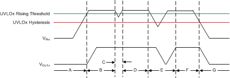 Figure 46. Typical UVLOx Operation
Table 5. Typical UVLOx Operation Description
| REGION | EVENT | VOUTx STATUS | COMMENT |
|---|---|---|---|
| A | Turn-on, VINx ≥ VUVLOx | 0 | Start-up |
| B | Regulation | 1 | Regulates to target VOUTx |
| C | Brownout, VINx ≥ VUVLOx – VHYS | 1 | The output can fall out of regulation but the device is still enabled. |
| D | Regulation | 1 | Regulates to target VOUTx |
| E | Brownout, VINx < VUVLOx – VHYS | 0 | The device is disabled and the output falls because of the load and active discharge circuit. The device is reenabled when the UVLOx rising threshold is reached by the input voltage and a normal start-up then follows. |
| F | Regulation | 1 | Regulates to target VOUTx |
| G | Turn-off, VINx < VUVLOx – VHYS | 0 | The output falls because of the load and active discharge circuit. |
Similar to many other LDOs with this feature, the UVLOx circuit takes a few microseconds to fully assert. During this time, a downward line transient below approximately 0.8 V causes the UVLOx to assert for a short time; however, the UVLOx circuit does not have enough stored energy to fully discharge the internal circuits inside of the device. When the UVLOx circuit is not given enough time to fully discharge the internal nodes, the outputs are not fully disabled.
The effect of the downward line transient can be mitigated by using a larger input capacitor to increase the fall time of the input supply when operating near the minimum VINx.
8.1.2.3 Power-Good (PGx) Function
The power-good circuit monitors the voltage at the feedback pin to indicate the status of the output voltage. The power-good circuit asserts whenever FBx, VINx, or ENx are below their thresholds. The PGx operation versus the output voltage is shown in Figure 47, which is described by Table 6.
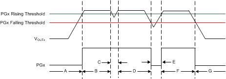 Figure 47. Typical PGx Operation
Table 6. Typical PGx Operation Description
| REGION | EVENT | PGx STATUS | FBx VOLTAGE |
|---|---|---|---|
| A | Turn-on | 0 | VFBx < VIT(PGx) + VHYS(PGx) |
| B | Regulation | Hi-Z | VFBx ≥ VIT(PGx) |
| C | Output voltage dip | Hi-Z | |
| D | Regulation | Hi-Z | |
| E | Output voltage dip | 0 | VFBx < VIT(PGx) |
| F | Regulation | Hi-Z | VFBx ≥ VIT(PGx) |
| G | Turn-off | 0 | VFBx < VIT(PGx) |
The PGx pin is open-drain and connecting a pullup resistor to an external supply enables others devices to receive power-good as a logic signal that can be used for sequencing. Make sure that the external pullup supply voltage results in a valid logic signal for the receiving device or devices.
To ensure proper operation of the power-good circuit, the pullup resistor value must be between 10 kΩ and 100 kΩ. The lower limit of 10 kΩ results from the maximum pulldown strength of the power-good transistor, and the upper limit of 100 kΩ results from the maximum leakage current at the power-good node. If the pullup resistor is outside of this range, then the power-good signal may not read a valid digital logic level.
Using a large CFFx with a small CNR/SSx causes the power-good signal to incorrectly indicate that the output voltage has settled during turn-on. The CFFx time constant must be greater than the soft-start time constant to ensure proper operation of the PGx during start-up. For a detailed description, see the Pros and Cons of Using a Feed-Forward Capacitor with a Low Dropout Regulator application report (SBVA042).
The state of PGx is only valid when the device operates above the minimum supply voltage. During short brownout events and at light loads, power-good does not assert because the output voltage (therefore VFBx) is sustained by the output capacitance.
8.1.3 AC and Transient Performance
LDO ac performance for a dual-channel device includes power-supply rejection ratio, channel-to-channel output isolation, output current transient response, and output noise. These metrics are primarily a function of open-loop gain, bandwidth, and phase margin that control the closed-loop input and output impedance of the LDO. The output noise is primarily a result of the reference and error amplifier noise.
8.1.3.1 Power-Supply Rejection Ratio (PSRR)
PSRR is a measure of how well the LDO control-loop rejects signals from VINx to VOUTx across the frequency spectrum (usually 10 Hz to 10 MHz). Equation 6 gives the PSRR calculation as a function of frequency for the input signal [VINx(f)] and output signal [VOUTx(f)].

Even though PSRR is a loss in signal amplitude, PSRR is shown as positive values in decibels (dB) for convenience.
A simplified diagram of PSRR versus frequency is shown in Figure 48.
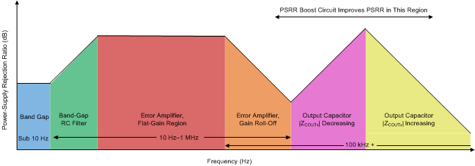 Figure 48. Power-Supply Rejection Ratio Diagram
An LDO is often employed not only as a dc-dc regulator, but also to provide exceptionally clean power-supply voltages that exhibit ultra-low noise and ripple to sensitive system components. This usage is especially true for the TPS7A87.
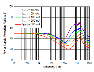
The TPS7A87 features an innovative circuit to boost the PSRR between 200 kHz and 1 MHz; see Figure 4. To achieve the maximum benefit of this PSRR boost circuit, using a capacitor with a minimum impedance in the 100-kHz to 1-MHz band is recommended.
8.1.3.2 Channel-to-Channel Output Isolation and Crosstalk
Output isolation is a measure of how well the device prevents voltage disturbances on one output from affecting the other output. This attenuation appears in load transient tests on the other output; however, to numerically quantify the rejection, the output channel isolation is expressed in decibels (dB).
Output isolation performance is a strong function of the PCB layout. See the Layout section on how to best optimize the isolation performance.
8.1.3.3 Output Voltage Noise
The TPS7A87 is designed for system applications where minimizing noise on the power-supply rail is critical to system performance. For example, the TPS7A87 can be used in a phase-locked loop (PLL)-based clocking circuit can be used for minimum phase noise, or in test and measurement systems where even small power-supply noise fluctuations reduce system dynamic range.
LDO noise is defined as the internally-generated intrinsic noise created by the semiconductor circuits alone. This noise is the sum of various types of noise (such as shot noise associated with current-through-pin junctions, thermal noise caused by thermal agitation of charge carriers, flicker noise, or 1/f noise and dominates at lower frequencies as a function of 1/f). Figure 49 shows a simplified output voltage noise density plot versus frequency.
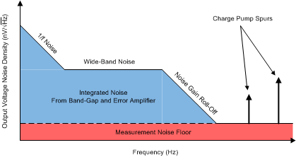 Figure 49. Output Voltage Noise Diagram
For further details, see the How to Measure LDO Noise white paper (SLYY076).
8.1.3.4 Optimizing Noise and PSRR
The ultra-low noise floor and PSRR of the device can be improved in several ways, as described in Table 7.
Table 7. Effect of Various Parameters on AC Performance(1)(2)
| PARAMETER | NOISE | PSRR | ||||
|---|---|---|---|---|---|---|
| LOW-FREQUENCY | MID-FREQUENCY | HIGH-FREQUENCY | LOW-FREQUENCY | MID-FREQUENCY | HIGH-FREQUENCY | |
| CNR/SSx | +++ | No effect | No effect | +++ | + | No effect |
| CFFx | ++ | +++ | + | ++ | +++ | + |
| COUTx | No effect | + | +++ | No effect | + | +++ |
| VINx – VOUTx | + | + | + | +++ | +++ | ++ |
| PCB layout | ++ | ++ | + | + | +++ | +++ |
The noise-reduction capacitor, in conjunction with the noise-reduction resistor, forms a low-pass filter (LPF) that filters out the noise from the reference before being gained up with the error amplifier, thereby minimizing the output voltage noise floor. The LPF is a single-pole filter and the cutoff frequency can be calculated with Equation 7. The typical value of RNR is 250 kΩ. The effect of the CNR/SSx capacitor increases when VOUTx(Target) increases because the noise from the reference is gained up when the output voltage increases. For low-noise applications, a 10-nF to 10-µF CNR/SSx is recommended.
The feed-forward capacitor reduces output voltage noise by filtering out the mid-band frequency noise. The feed-forward capacitor can be optimized by placing a pole-zero pair near the edge of the loop bandwidth and pushing out the loop bandwidth, thus improving mid-band PSRR.
A larger COUTx or multiple output capacitors reduces high-frequency output voltage noise and PSRR by reducing the high-frequency output impedance of the power supply.
Additionally, a higher input voltage improves the noise and PSRR because greater headroom is provided for the internal circuits. However, a high power dissipation across the die increases the output noise because of the increase in junction temperature.
Good PCB layout improves the PSRR and noise performance by providing heatsinking at low frequencies and isolating VOUTx at high frequencies.
Table 8 lists the output voltage noise for the 10-Hz to 100-kHz band at a 5-V output for a variety of conditions with an input voltage of 5.4 V, an R1x of 12.1 kΩ, and a load current of 0.5 A. The 5-V output is chosen because this output is the worst-case condition for output voltage noise.
Table 8. Output Noise Voltage at a 5-V Output with a 5.4-V Input
| CNR/SSx (nF) | CFFx (nF) | COUTx (µF) | SS_CTRLx | OUTPUT VOLTAGE NOISE (µVRMS) |
|---|---|---|---|---|
| 10 | 10 | 22 | VINx | 10.8 |
| 1000 | 100 | 22 | VINx | 5.6 |
| 1000 | 100 | 22 | GND | 5.6 |
| 1000 | 100 | 22 || 1000 | VINx | 5.0 |
8.1.3.4.1 Charge Pump Noise
The device internal charge pump generates a minimal amount of noise.
The high-frequency components of the output voltage noise density curve are filtered out in most applications by using 10-nF to 100-nF bypass capacitors close to the load. Using a ferrite bead between the LDO output and the load input capacitors forms a pi-filter, further reducing the high-frequency noise contribution.
8.1.3.5 Load Transient Response
The load-step transient response is the output voltage response by the LDO to a step in load current, whereby output voltage regulation is maintained. There are two key transitions during a load transient response: the transition from a light to a heavy load and the transition from a heavy to a light load. The regions shown in Figure 50 are broken down in this section and are described in Table 9. Regions A, E, and H are where the output voltage is in steady-state.
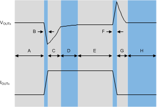 Figure 50. Load Transient Waveform
Table 9. Load Transient Waveform Description
| REGION | DESCRIPTION | COMMENT |
|---|---|---|
| A | Regulation | Regulation |
| B | Output current ramping | Initial voltage dip is a result of the depletion of the output capacitor charge. |
| C | LDO responding to transient | Recovery from the dip results from the LDO increasing its sourcing current, and leads to output voltage regulation. |
| D | Reaching thermal equilibrium | At high load currents the LDO takes some time to heat up. During this time the output voltage changes slightly. |
| E | Regulation | Regulation |
| F | Output current ramping | Initial voltage rise results from the LDO sourcing a large current, and leads to the output capacitor charge to increase. |
| G | LDO responding to transient | Recovery from the rise results from the LDO decreasing its sourcing current in combination with the load discharging the output capacitor. |
| H | Regulation | Regulation |
The transient response peaks (VOUTx(max) and VOUTx(min)) are improved by using more output capacitance; however, doing so slows down the recovery time (Wrise and Wfall). Figure 51 shows these parameters during a load transient, with a given pulse duration (PW) and current levels (IOUTx(LO) and IOUTx(HI)).
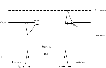 Figure 51. Simplified Load Transient Waveform
8.1.4 DC Performance
8.1.4.1 Output Voltage Accuracy (VOUTx)
The device features an output voltage accuracy of 1% maximum that includes the errors introduced by the internal reference, load regulation, line regulation, and operating temperature as specified by the Electrical Characteristics table. Output voltage accuracy specifies minimum and maximum output voltage error, relative to the expected nominal output voltage stated as a percent.
8.1.4.2 Dropout Voltage (VDO)
Generally speaking, the dropout voltage often refers to the minimum voltage difference between the input and output voltage (VDO = VINx – VOUTx) that is required for regulation. When VINx drops below the required VDO for the given load current, the device functions as a resistive switch and does not regulate output voltage. Dropout voltage is proportional to the output current because the device is operating as a resistive switch, as shown in Figure 52.
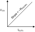 Figure 52. Dropout Voltage versus Output Current
Dropout voltage is affected by the drive strength for the gate of the pass element, which is nonlinear with respect to VINx on this device because of the internal charge pump. Dropout voltage increases exponentially when the input voltage nears its maximum operating voltage because the charge pump multiplies the input voltage by a factor of 4 and then is internally clamped to 8.0 V.
8.1.4.2.1 Behavior when Transitioning from Dropout into Regulation
Some applications can have transients that place the LDO into dropout, such as slower ramps on VINX for start-up or load transients. As with many other LDOs, the output can overshoot on recovery from these conditions.
A ramping input supply can cause an LDO to overshoot on start-up when the slew rate and voltage levels are in the right range, as shown in Figure 53. This condition is easily avoided through either the use of an enable signal, or by increasing the soft-start time with CSS/NRx.
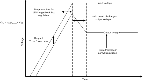 Figure 53. Start-Up Into Dropout
8.1.5 Reverse Current Protection
As with most LDOs, this device can be damaged by excessive reverse current.
Reverse current is current that flows through the body diode on the pass element instead of the normal conducting channel. This current flow, at high enough magnitudes, degrades long-term reliability of the device resulting from risks of electromigration and excess heat being dissipated across the device. If the current flow gets high enough, a latch-up condition can be entered.
Conditions where excessive reverse current can occur are outlined in this section, all of which can exceed the absolute maximum rating of VOUTx > VINx + 0.3 V:
- If the device has a large COUTx and the input supply collapses quickly with little or no load current
- The output is biased when the input supply is not established
- The output is biased above the input supply
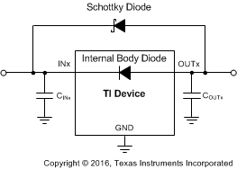 Figure 54. Example Circuit for Reverse Current Protection Using a Schottky Diode
8.1.6 Power Dissipation (PD)
Circuit reliability demands that proper consideration is given to device power dissipation, location of the circuit on the printed circuit board (PCB), and correct sizing of the thermal plane. The PCB area around the regulator must be as free as possible of other heat-generating devices that cause added thermal stresses.
As a first-order approximation, power dissipation in the regulator depends on the input-to-output voltage difference and load conditions. PD can be approximated using Equation 8:
An important note is that power dissipation can be minimized, and thus greater efficiency achieved, by proper selection of the system voltage rails. Proper selection allows the minimum input-to-output voltage differential to be obtained. The low dropout of the device allows for maximum efficiency across a wide range of output voltages.
The main heat conduction path for the device is through the thermal pad on the package. As such, the thermal pad must be soldered to a copper pad area under the device. This pad area contains an array of plated vias that conduct heat to any inner plane areas or to a bottom-side copper plane.
The maximum power dissipation determines the maximum allowable junction temperature (TJ) for the device. Power dissipation and junction temperature are most often related by the junction-to-ambient thermal resistance (θJA) of the combined PCB, device package, and the temperature of the ambient air (TA), according to Equation 9. The equation is rearranged for output current in Equation 10.
Unfortunately, this thermal resistance (θJA) is highly dependent on the heat-spreading capability built into the particular PCB design, and therefore varies according to the total copper area, copper weight, and location of the planes. The θJA recorded in the table is determined by the JEDEC standard, PCB, and copper-spreading area, and is only used as a relative measure of package thermal performance. Note that for a well-designed thermal layout, θJA is actually the sum of the VQFN package junction-to-case (bottom) thermal resistance (θJCbot) plus the thermal resistance contribution by the PCB copper.
8.1.6.1 Estimating Junction Temperature
The JEDEC standard now recommends the use of psi (Ψ) thermal metrics to estimate the junction temperatures of the LDO when in-circuit on a typical PCB board application. These metrics are not strictly speaking thermal resistances, but rather offer practical and relative means of estimating junction temperatures. These psi metrics are determined to be significantly independent of the copper-spreading area. The key thermal metrics (ΨJT and ΨJB) are given in the table and are used in accordance with Equation 11.

where
- PD is the power dissipated as explained in Equation 8
- TT is the temperature at the center-top of the device package, and
- TB is the PCB surface temperature measured 1 mm from the device package and centered on the package edge
8.1.6.2 Recommended Area for Continuous Operation (RACO)
The operational area of an LDO is limited by the dropout voltage, output current, junction temperature, and input voltage. The recommended area for continuous operation for a linear regulator can be separated into the following parts, and is shown in Figure 55:
- Limited by dropout: Dropout voltage limits the minimum differential voltage between the input and the output (VINx – VOUTx) at a given output current level; see the Dropout Voltage (VDO) section for more details.
- Limited by rated output current: The rated output current limits the maximum recommended output current level. Exceeding this rating causes the device to fall out of specification.
- Limited by thermals: The shape of the slope is given by Equation 10. The slope is nonlinear because the junction temperature of the LDO is controlled by the power dissipation across the LDO; therefore, when VINx – VOUTx increases, the output current must decrease in order to ensure that the rated junction temperature of the device is not exceeded. Exceeding this rating can cause the device to fall out of specifications and reduces long-term reliability.
- Limited by VINx range: The rated input voltage range governs both the minimum and maximum of VINx – VOUTx.
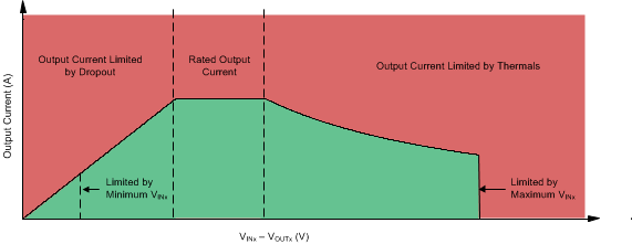 Figure 55. Continuous Operation Slope Region Description
Figure 56 to Figure 61 show the recommended area of operation curves for this device on a JEDEC-standard, high-K board with a θJA = 35.4°C/W, as given in the table.
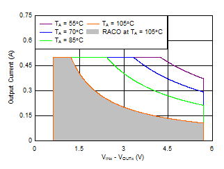 Figure 56. Recommended Area for Continuous Operation for VOUTx = 0.8 V
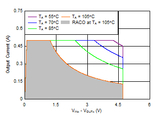 Figure 58. Recommended Area for Continuous Operation for VOUTx = 1.8 V
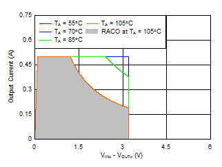 Figure 60. Recommended Area for Continuous Operation for VOUTx = 3.3 V
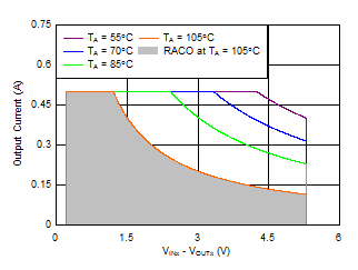 Figure 57. Recommended Area for Continuous Operation for VOUTx = 1.2 V
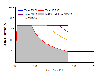 Figure 59. Recommended Area for Continuous Operation for VOUTx = 2.5 V
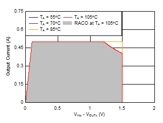 Figure 61. Recommended Area for Continuous Operation for VOUTx = 5.0 V
8.2 Typical Application
This section discusses the implementation of the TPS7A87 to regulate from a common input voltage to two output voltages of the same value. This application is common for when two noise-sensitive loads must have the same supply voltage but have high channel-to-channel isolation. The schematic for this application circuit is provided in Figure 62.
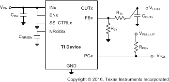 Figure 62. Application Example (Single Channel)
8.2.1 Design Requirements
For the design example shown in Figure 62, use the parameters listed in Table 10 as the input parameters.
Table 10. Design Parameters
| PARAMETER | DESIGN REQUIREMENT |
|---|---|
| Input voltages (VIN1 and VIN2) | 1.8 V, ±3%, provided by the dc-dc converter switching at 750 kHz |
| Maximum ambient operating temperature | 85°C |
| Output voltages (VOUT1 and VOUT2) | 1.2 V, ±1%, output voltages are isolated |
| Output currents (IOUT2 and IOUT2) | 400 mA (maximum), 10 mA (minimum) |
| Channel-to-channel isolation | Isolation greater than 50 dB at 100 kHz |
| RMS noise | < 5 µVRMS, bandwidth = 10 Hz to 100 kHz |
| PSRR at 750 kHz | > 40 dB |
| Startup time | < 5 ms |
8.2.2 Detailed Design Procedure
The output voltages can be set to 1.2 V by selecting the correct values for R1x and R2x; see Equation 1.
Input and output capacitors are selected in accordance with the External Component Selection section. Ceramic capacitances of 10 µF for both inputs and outputs are selected.
To minimize noise, a feed-forward capacitance (CFFx) of 10 nF is selected.
Channel-to-channel isolation depends greatly on the layout of the design. To minimize crosstalk between the outputs, keep the output capacitor grounds on separate sides of the design. See the Layout section for an example of how to layout the TPS7A87 to achieve best PSRR, channel-to-channel isolation, and noise.
8.2.3 Application Curves
