SBVS289A August 2017 – September 2017 TPS7A88-Q1
PRODUCTION DATA.
- 1 Features
- 2 Applications
- 3 Description
- 4 Revision History
- 5 Pin Configuration and Functions
- 6 Specifications
- 7 Detailed Description
- 8 Application and Implementation
- 9 Power Supply Recommendations
- 10Layout
- 11Device and Documentation Support
- 12Mechanical, Packaging, and Orderable Information
Package Options
Refer to the PDF data sheet for device specific package drawings
Mechanical Data (Package|Pins)
- RTJ|20
Thermal pad, mechanical data (Package|Pins)
Orderable Information
5 Pin Configuration and Functions
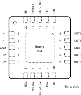
RTJ Package
20-Pin WQFN With Exposed Thermal Pad
Top View

Pin Functions
| PIN | DESCRIPTION | ||
|---|---|---|---|
| NAME | NO. | I/O | |
| EN1 | 20 | I | Enable pin for each channel. These pins turn the regulator on and off. If VENx(1) ≥ VIH(ENx), then the regulator is enabled. If VENx ≤ VIL(ENx), then the regulator is disabled. The ENx pin must be connected to INx if the enable function is not used. |
| EN2 | 6 | ||
| FB1 | 16 | I | Feedback pins connected to the error amplifier. Although not required, a TI recommends a 10-nF feedforward capacitor from FBx to OUTx (as close as possible to the device) to maximize AC performance. The use of a feedforward capacitor can disrupt PGx (power good) functionality. See Feedforward Capacitor (CFFx) and Setting the Output Voltage (Adjustable Operation) for more details. |
| FB2 | 10 | ||
| GND | 3, 13 | — | Ground pins. These pins must be connected to ground, the thermal pad, and each other with a low-impedance connection. |
| IN1 | 1, 2 | I | Input supply pins for LDO 1. An input capacitor with a value of 10 µF or larger (5 µF or greater of effective capacitance) is required. Place the input capacitor as close as possible to the input. |
| IN2 | 4, 5 | I | Input supply pins for LDO 2. An input capacitor with a value of 10 µF or larger (5 µF or greater of effective capacitance) is required. Place the input capacitor as close as possible to the input. |
| NR/SS1 | 19 | — | Noise-reduction and soft-start pin for each channel. Connecting an external capacitor between this pin and ground reduces reference voltage noise and enables the soft-start function. Although not required, TI recommends connecting a capacitor with a value of 10 nF or larger from NR/SSx to GND (as close as possible to the pin) to maximize AC performance. See Noise-Reduction and Soft-Start Capacitor (CNR/SSx) for more details. |
| NR/SS2 | 7 | ||
| OUT1 | 14, 15 | O | Regulated outputs for LDO 1. A ceramic capacitor with a value of 5 µF or larger (10 μF or greater of effective capacitance) from OUTx to ground is required for stability and must be placed as close as possible to the output. Minimize the impedance from the OUT1 pin to the load. See Input and Output Capacitor (CINx and COUTx) for more details. |
| OUT2 | 11, 12 | O | Regulated outputs for LDO 2. A ceramic capacitor with a value of 10 µF or larger (5 μF or greater of effective capacitance) from OUTx to ground is required for stability and must be placed as close as possible to the output. Minimize the impedance from the OUT2 pin to the load. See Input and Output Capacitor (CINx and COUTx) for more details. |
| PG1 | 17 | O | Open-drain power-good indicator pins for the LDO 1 and LDO 2 output voltages. A 10-kΩ to 100-kΩ external pullup resistor is required. These pins can be left floating or connected to GND if not used. The use of a feedforward capacitor can disrupt power-good functionality. See Feedforward Capacitor (CFFx) for more details. |
| PG2 | 9 | ||
| SS_CTRL1 | 18 | I | Soft-start control pins for each channel. Connect these pins to GND or INx to allow normal or fast charging of the NR/SSx capacitor. If a CNR/SSx capacitor is not used, SS_CTRLx must be connected to GND to avoid output overshoot. |
| SS_CTRL2 | 8 | ||
| Thermal pad | — | Connect the thermal pad to a large-area ground plane. The thermal pad is internally connected to GND. | |
(1) Lowercase x indicates that the specification under consideration applies to both channel 1 and channel 2, one channel at a time.