SLVSDN3 June 2017 TPS82140
PRODUCTION DATA.
- 1 Features
- 2 Applications
- 3 Description
- 4 Revision History
- 5 Pin Configuration and Functions
- 6 Specifications
- 7 Detailed Description
- 8 Application and Implementation
- 9 Power Supply Recommendations
- 10Layout
- 11Device and Documentation Support
- 12Mechanical, Packaging, and Orderable Information
Package Options
Mechanical Data (Package|Pins)
- SIL|8
Thermal pad, mechanical data (Package|Pins)
Orderable Information
8 Application and Implementation
NOTE
Information in the following applications sections is not part of the TI component specification, and TI does not warrant its accuracy or completeness. TI’s customers are responsible for determining suitability of components for their purposes. Customers should validate and test their design implementation to confirm system functionality.
8.1 Application Information
The output voltage of the TPS82140 is adjusted by component selection. The following section discusses the design of the external components to complete the power supply design for several input and output voltage options by using typical applications as a reference.
8.2 Typical Applications
8.2.1 1.8-V Output Application
space
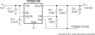 Figure 5. 1.8-V Output Application
8.2.1.1 Design Requirements
For this design example, use the following as the input parameters.
Table 2. Design Parameters
| DESIGN PARAMETER | EXAMPLE VALUE |
|---|---|
| Input voltage range | 12V |
| Output voltage | 1.8V |
| Output ripple voltage | < 20mV |
| Output current rating | 2A |
The components used for measurements are given in the following table.
Table 3. List of Components
| REFERENCE | DESCRIPTION(1) | MANUFACTURER |
|---|---|---|
| C1 | 10 µF, 25 V, X7R, ±20%, size 1206, C3216X7R1E106M160AE | TDK |
| C2 | 22 µF, 10 V, X7S, ±20%, size 0805, C2012X7S1A226M125AC | TDK |
| C3 | 3300 pF, 50 V, ±5%, C0G/NP0, size 0603, GRM1885C1H332JA01D | Murata |
| R1, R2, R3 | Standard |
8.2.1.2 Detailed Design Procedure
8.2.1.2.1 Custom Design with WEBENCH® Tools
Click here to create a custom design using the TPS82140 device with the WEBENCH® Power Designer.
- Start by entering your VIN, VOUT, and IOUT requirements.
- Optimize your design for key parameters like efficiency, footprint and cost using the optimizer dial and compare this design with other possible solutions from Texas Instruments.
- The WEBENCH Power Designer provides you with a customized schematic along with a list of materials with real time pricing and component availability.
- In most cases, you will also be able to:
- Run electrical simulations to see important waveforms and circuit performance
- Run thermal simulations to understand the thermal performance of your board
- Export your customized schematic and layout into popular CAD formats
- Print PDF reports for the design, and share your design with colleagues
- Get more information about WEBENCH tools at www.ti.com/WEBENCH.
8.2.1.2.2 Setting the Output Voltage
The output voltage is set by an external resistor divider according to the following equations:
space

space
R2 should not be higher than 100kΩ to achieve high efficiency at light load while providing acceptable noise sensitivity. Larger currents through R2 improve noise sensitivity and output voltage accuracy. Figure 5 shows the external resistor divider value for a 1.8-V output. Choose appropriate resistor values for other outputs.
In case the FB pin gets opened, the device clamps the output voltage at the VOUT pin internally to about 7V.
8.2.1.2.3 Input and Output Capacitor Selection
For best output and input voltage filtering, low ESR ceramic capacitors are required. The input capacitor minimizes input voltage ripple, suppresses input voltage spikes and provides a stable system rail for the device. A 10-µF or larger input capacitor is required. The output capacitor value can range from 22μF up to more than 400μF. Higher values are possible as well and can be evaluated through the transient response. Larger soft start times are recommended for higher output capacitances.
High capacitance ceramic capacitors have a DC Bias effect, which will have a strong influence on the final effective capacitance. Therefore the right capacitor value has to be chosen carefully. Package size and voltage rating in combination with dielectric material are responsible for differences between the rated capacitor value and the effective capacitance.
8.2.1.2.4 Soft Startup Capacitor Selection
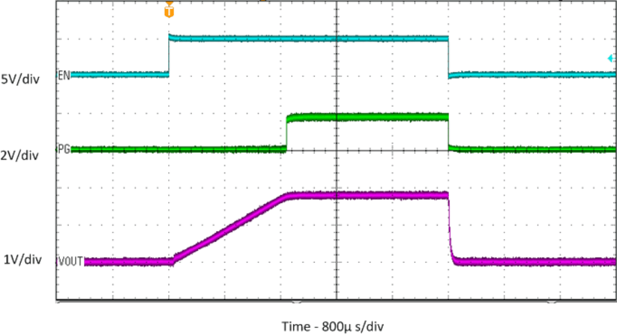
A capacitance connected between the SS/TR pin and the GND allows programming the startup slope of the output voltage. A constant current of 2.5 μA charges the external capacitor. The capacitance required for a given soft startup time for the output voltage is given by:
space

8.2.1.3 Application Performance Curves
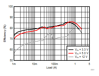
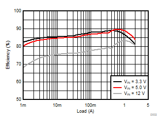
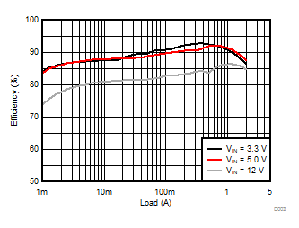
TA = 25°C, VIN = 12 V, VOUT = 1.8 V, unless otherwise noted.
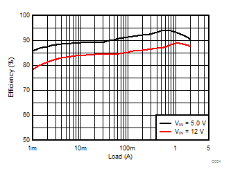
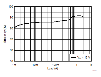
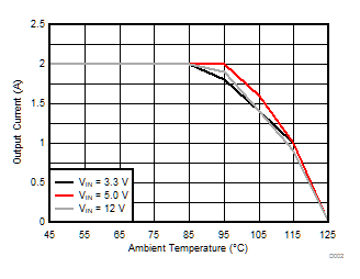
| θJA = 46.1 °C/W |
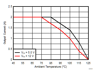
| θJA = 46.1 °C/W |
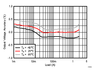
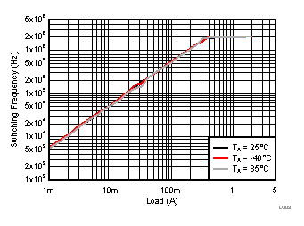
| VOUT = 1.8V |
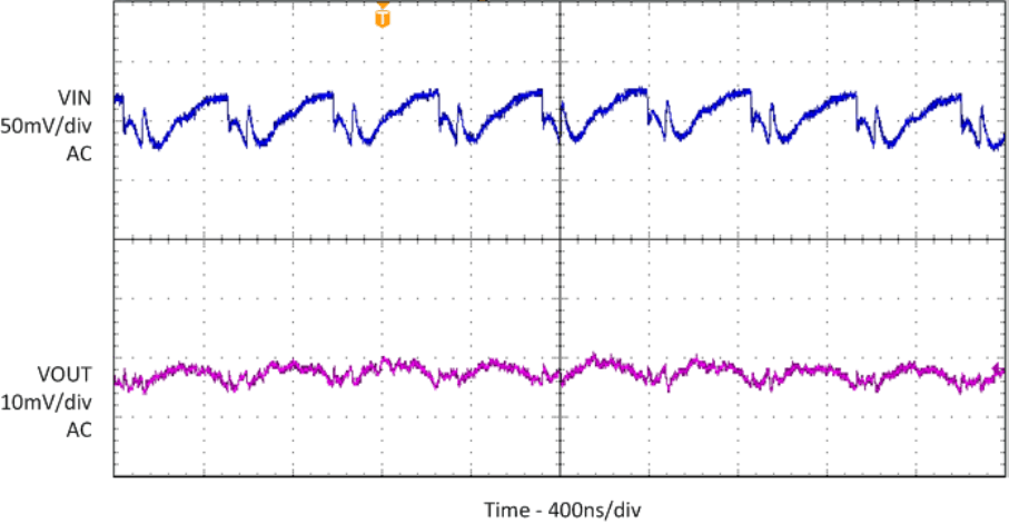
| IOUT = 2A |
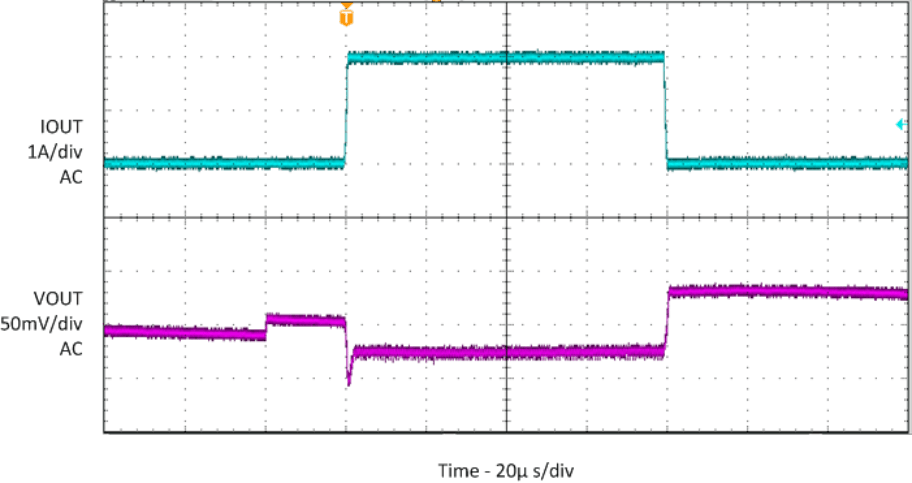
| IOUT = 0A to 2A, 1A/µs |
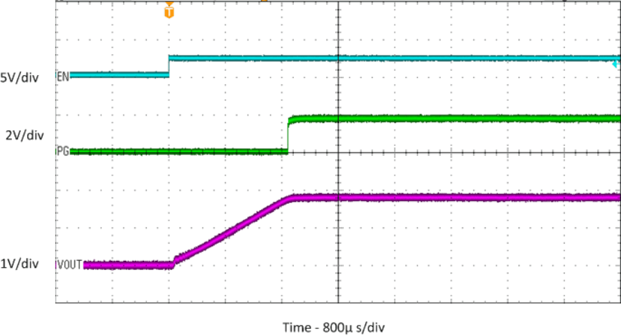
| No Load |
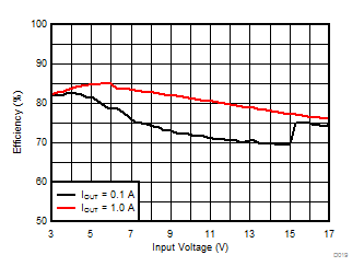
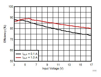
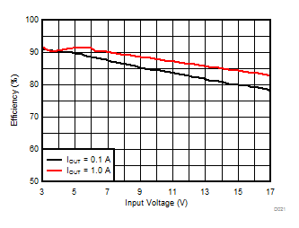
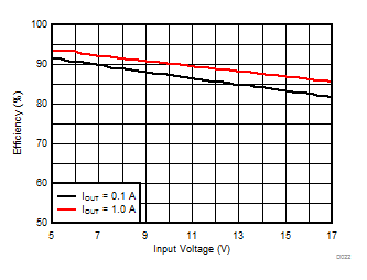
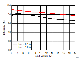
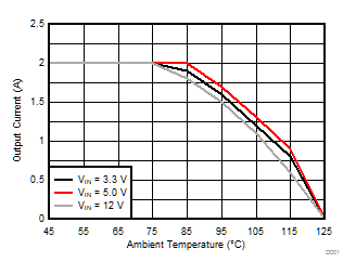
| θJA = 46.1 °C/W |
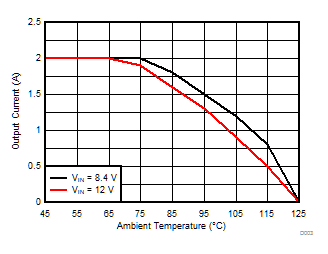
| θJA = 46.1 °C/W |
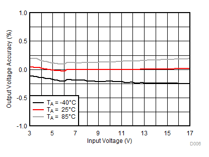
| IOUT = 1A |
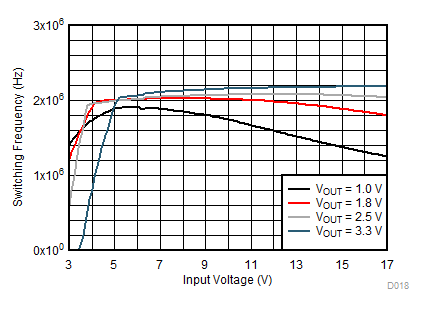
| IOUT = 1A |
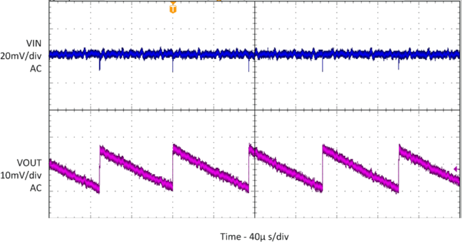
| No Load |
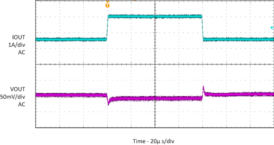
| IOUT = 0.5A to 2A, 1A/µs |
| ROUT = 1Ω |
8.3 System Examples
8.3.1 Inverting Power Supply
The TPS82140 can be used as inverting power supply by rearranging external circuitry as shown in Figure 30. As the former GND node now represents a voltage level below system ground, the voltage difference between VIN and VOUT has to be limited for operation to the maximum supply voltage of 17V (see Equation 8).
space

space
space
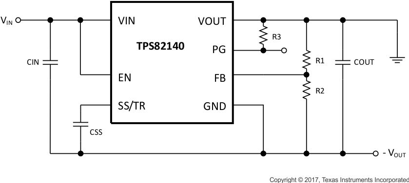 Figure 30. Inverting Power Supply Schematic
space
The transfer function of the inverting power supply configuration differs from the buck mode transfer function, incorporating a Right Half Plane Zero additionally. Therefore the loop stability has to be adapted. More detailed information is given in TIDUCV2.