SLVSBK3A December 2012 – September 2015 TPS92690
PRODUCTION DATA.
- 1 Features
- 2 Applications
- 3 Description
- 4 Revision History
- 5 Pin Configuration and Functions
- 6 Specifications
-
7 Detailed Description
- 7.1 Overview
- 7.2 Functional Block Diagram
- 7.3
Feature Description
- 7.3.1 Current Regulators
- 7.3.2 Peak Current Mode Control
- 7.3.3 Switching Frequency and Synchronization
- 7.3.4 Current Sense and Current Limit
- 7.3.5 Average LED Current
- 7.3.6 Precision Reference (VREF)
- 7.3.7 Low-Level Analog Dimming
- 7.3.8 Soft-Start and Shutdown
- 7.3.9 VCC Regulator and Start-Up
- 7.3.10 Overvoltage Protection (OVP)
- 7.3.11 Input Undervoltage Lockout (UVLO)
- 7.3.12 PWM Dimming
- 7.3.13 Control Loop Compensation
- 7.3.14 Thermal Shutdown
- 7.4 Device Functional Modes
-
8 Application and Implementation
- 8.1 Application Information
- 8.2
Typical Applications
- 8.2.1
Basic Topology Schematics
- 8.2.1.1 Design Requirements
- 8.2.1.2
Detailed Design Procedure
- 8.2.1.2.1 Operating Point
- 8.2.1.2.2 Switching Frequency
- 8.2.1.2.3 Average LED Current
- 8.2.1.2.4 Inductor Ripple Current
- 8.2.1.2.5 Output Capacitance
- 8.2.1.2.6 Peak Current Limit
- 8.2.1.2.7 Loop Compensation
- 8.2.1.2.8 Input Capacitance
- 8.2.1.2.9 NFET
- 8.2.1.2.10 Diode
- 8.2.1.2.11 Input UVLO
- 8.2.1.2.12 Output OVLO
- 8.2.1.3 Application Curve
- 8.2.2
Simplified Application
- 8.2.2.1 Design Requirements
- 8.2.2.2
Detailed Design Procedure
- 8.2.2.2.1 Operating Point
- 8.2.2.2.2 Switching Frequency
- 8.2.2.2.3 Average LED Current
- 8.2.2.2.4 Inductor Ripple Current
- 8.2.2.2.5 LED Ripple Current
- 8.2.2.2.6 Peak Current Limit
- 8.2.2.2.7 Loop Compensation
- 8.2.2.2.8 Input Capacitance
- 8.2.2.2.9 NFET
- 8.2.2.2.10 Diode
- 8.2.2.2.11 Output OVLO
- 8.2.2.2.12 Input UVLO
- 8.2.2.2.13 Soft-Start
- 8.2.2.2.14 PWM Dimming Method
- 8.2.2.2.15 Analog Dimming Method
- 8.2.1
Basic Topology Schematics
- 9 Power Supply Recommendations
- 10Layout
- 11Device and Documentation Support
- 12Mechanical, Packaging, and Orderable Information
Package Options
Mechanical Data (Package|Pins)
- PWP|16
Thermal pad, mechanical data (Package|Pins)
- PWP|16
Orderable Information
1 Features
- Input Voltage Range from 4.5 to 75 V
- Adjustable Current Sense (50 to 500 mV)
- Low-Side Current Sensing
- 2-Ω MOSFET Gate Driver
- Input Undervoltage Protection
- Output Overvoltage Protection
- Cycle-by-Cycle Current Limit
- PWM Dimming Input
- Programmable Oscillator Frequency
- External Synchronization Capability
- Slope Compensation
- Programmable Soft-Start Function
- HTSSOP (PWP), 16-Pin, Exposed Pad Package
2 Applications
- LED Drivers
- Constant Current Regulator: Boost, Cuk, Flyback, and SEPIC
3 Description
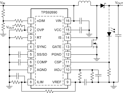
The TPS92690 device is a high-voltage, low-side NFET controller with an adjustable output current sense resistor voltage. Ideal for LED drivers, it contains all of the features needed to implement current regulators based on boost, SEPIC, flyback, and Cuk topologies.
Output current regulation is based on peak current-mode control supervised by a control loop. This methodology eases the design of loop compensation while providing inherent input voltage feed-forward compensation. The TPS92690 device includes a high-voltage start-up regulator that operates over a wide input range between 4.5 and 75 V. The PWM controller is designed for high-speed capability including an oscillator frequency range up to 2 MHz. The TPS92690 device includes an error amplifier, precision reference, cycle-by-cycle current limit, and thermal shutdown.
Device Information(1)
| PART NUMBER | PACKAGE | BODY SIZE (NOM) |
|---|---|---|
| TPS92690 | HTSSOP (16) | 5.00 mm × 4.40 mm |
- For all available packages, see the orderable addendum at the end of the data sheet.
Simplified Application
