SLUSCV7A July 2017 – August 2017 TPSM84203 , TPSM84205 , TPSM84212
PRODUCTION DATA.
- 1 Features
- 2 Applications
- 3 Description
- 4 Revision History
- 5 Pin Configuration and Functions
- 6 Specifications
- 7 Detailed Description
- 8 Application and Implementation
- 9 Power Supply Recommendations
- 10Layout
- 11Device and Documentation Support
- 12Mechanical, Packaging, and Orderable Information
Package Options
Mechanical Data (Package|Pins)
- EAB|3
Thermal pad, mechanical data (Package|Pins)
Orderable Information
7 Detailed Description
7.1 Overview
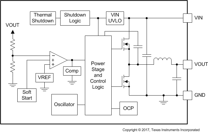
The TPSM84203, TPSM84205, and TPSM84212 devices are 28 V input, 1.5 A, synchronous step down converters with PWM, MOSFETs, inductor, and control circuitry integrated into a TO-220 footprint package. The device integration enables small designs, while improving efficiency over a traditional linear regulator design. The TPSM842xx family provides fixed output voltages of 3.3 V, 5.0 V and 12.0 V. The fixed 400 kHz (typ) switching frequency allows small size and low output voltage ripple. Under light load conditions, these devices are designed to operate in high-efficiency pulse-skipping mode. These devices provide accurate voltage regulation for a variety of loads by using a precision internal voltage reference. These devices have been designed to safely start up into a pre-biased output voltage. Thermal shutdown and current limit features protect the device during an overload condition. The 3-pin, TO-220 footprint package offers improved performance over traditional linear regulators packaged in the standard footprint.
7.2 Functional Block Diagram
7.3 Feature Description
7.3.1 Input Capacitors
The TPSM842xx devices require a minimum input capacitance of 10 μF of ceramic type. High-quality ceramic type X5R or X7R capacitors with sufficient voltage rating are recommended. An additional 100 μF of non-ceramic capacitance is recommended for applications with transient load requirements. The voltage rating of input capacitors must be greater than the maximum input voltage.
Table 1. Recommended Input Capacitors(1)
| VENDOR | SERIES | PART NUMBER | CAPACITOR CHARACTERISTICS | ||
|---|---|---|---|---|---|
| WORKING VOLTAGE (V) |
CAPACITANCE (3)
(µF) |
ESR(2)
(mΩ) |
|||
| Murata | X7R | GRM32ER71H475KA88L | 50 | 4.7 | 2 |
| TDK | X5R | C3225X5R1H106K250AB | 50 | 10 | 3 |
| Murata | X7R | GRM32ER71H106KA12 | 50 | 10 | 2 |
| TDK | X7R | C3225X7R1H106M250AB | 50 | 10 | 3 |
| Panasonic | ZA | EEHZA1H101P | 50 | 100 | 28 |
7.3.2 Output Capacitors
The TPSM84203 and TPSM84205 devices require a minimum output capacitance of 94 μF (2x 47 μF) of ceramic type. The TPSM84212 device requires a minimum output capacitance of 47 μF of ceramic type. High-quality X5R or X7R ceramic capacitors with sufficient voltage rating are recommended. Additional output capacitance is recommended for applications with transient load requirements. The voltage rating of output capacitors must be greater than the maximum output voltage.
Table 2. Recommended Output Capacitors(1)
| VENDOR | SERIES | PART NUMBER | CAPACITOR CHARACTERISTICS | ||
|---|---|---|---|---|---|
| WORKING VOLTAGE (V) |
CAPACITANCE (1)
(µF) |
ESR(2)
(mΩ) |
|||
| TDK | X5R | C3225X5R0J476K | 6.3 | 47 | 2 |
| Murata | X5R | GRM32ER61C476K | 16 | 47 | 3 |
| TDK | X5R | C3225X5R0J107M | 6.3 | 100 | 2 |
| Murata | X5R | GRM32ER60J107M | 6.3 | 100 | 2 |
| Murata | X5R | GRM32ER61A107M | 10 | 100 | 2 |
| Kemet | X5R | C1210C107M4PAC7800 | 16 | 100 | 2 |
| Panasonic | POSCAP | 6TPE100MI | 6.3 | 100 | 18 |
| Panasonic | POSCAP | 6TPF220M9L | 6.3 | 220 | 9 |
| Panasonic | POSCAP | 6TPE220ML | 6.3 | 220 | 12 |
| Panasonic | POSCAP | 6TPF330M9L | 6.3 | 330 | 9 |
| Panasonic | POSCAP | 16TQC47MYFD | 16 | 47 | 55 |
7.3.3 Drop-Out Voltage
The drop-out voltage of a voltage regulator is the difference between the input voltage and the output voltage that is required to maintain regulation. Figure 16 and Figure 17 show typical drop-out voltage graphs for TPSM84205 at ambient temperatures of 25°C and 85°C. Figure 18 and Figure 19 show typical drop-out voltage graphs for TPSM84212 at ambient temperatures of 25°C and 85°C.
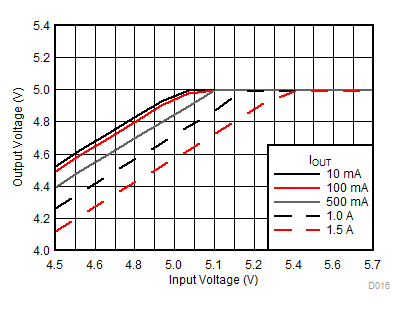
| VOUT = 5.0 V | TA = 25°C |
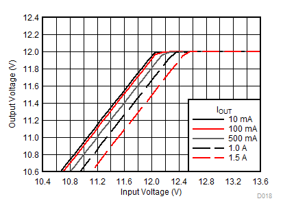
| VOUT = 12 V | TA = 25°C |
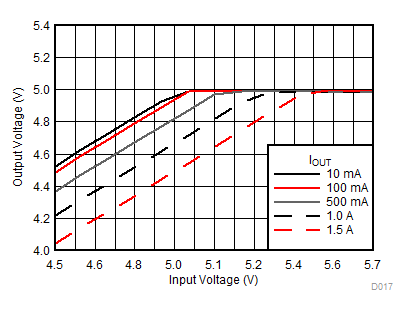
| VOUT = 5.0 V | TA = 85°C |
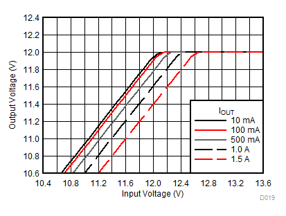
| VOUT = 12 V | TA = 85°C |
7.3.4 Internal Soft-Start
The device starts up under control of the internal soft-start function. The internal soft start time is set to 5 ms typically.
7.3.5 Safe Startup into Pre-Biased Outputs
The device has been designed to prevent the low-side MOSFET from discharging a pre-biased output. During monotonic pre-biased startup, both high-side and low-side MOSFETs are not allowed to be turned on until the internal soft-start voltage is higher than the internal feedback voltage.
7.3.6 Over-Current Protection
The device is protected from overcurrent conditions by cycle-by-cycle current limiting. If an output overload condition occurs for more than 1.28 ms, the device shuts down and restarts after approximately 40 ms. The hiccup mode helps to reduce the device power dissipation under severe overcurrent conditions.
7.3.7 Output Over-Voltage Protection
An output over voltage protection circuit is incorporated to minimize output voltage overshoot when recovering from output fault conditions or strong unload transients. When the output voltage goes above 108% × VOUT, the high-side MOSFET is forced off. When the output voltage falls below 104% × VOUT, the high-side MOSFET is enabled again.
7.3.8 Thermal Shutdown
The internal thermal-shutdown circuitry forces the device to stop switching if the junction temperature exceeds 165°C typically. The device reinitiates the power-up sequence when the junction temperature drops below 155°C typically.
7.4 Device Functional Modes
7.4.1 Normal Operation
The TPSM842xx devices operate in Normal operation mode when the input voltage is above the minimum input voltage. In Normal operation mode, the device operates in continuous conduction mode (CCM) which occurs when inductor peak current is above 840 mA typically. In CCM, the TPSM842xx devices operate at a fixed frequency of 400 kHz (typ). In addition, to reduce EMI, the devices introduce frequency spread spectrum. The jittering frequency range is ±6% of the switching frequency with a 780 Hz modulation rate.
7.4.2 Eco-mode™ Operation
The TPSM842xx devices operate in Eco-mode operation in light load conditions. Eco-mode is a high-efficiency, pulse-skipping mode under light load conditions. Pulse skipping initiates when the switch current falls to 840 mA typically. During pulse skipping, the low-side FET turns off when the switch current falls to 0 A. The device takes on the characteristics of discontinuous conduction mode (DCM) operation and the apparent switching frequency decreases. As the output current decreases, the perceived time between switching pulses increases.