SLUSCV7A July 2017 – August 2017 TPSM84203 , TPSM84205 , TPSM84212
PRODUCTION DATA.
- 1 Features
- 2 Applications
- 3 Description
- 4 Revision History
- 5 Pin Configuration and Functions
- 6 Specifications
- 7 Detailed Description
- 8 Application and Implementation
- 9 Power Supply Recommendations
- 10Layout
- 11Device and Documentation Support
- 12Mechanical, Packaging, and Orderable Information
Package Options
Mechanical Data (Package|Pins)
- EAB|3
Thermal pad, mechanical data (Package|Pins)
Orderable Information
8 Application and Implementation
NOTE
Information in the following applications sections is not part of the TI component specification, and TI does not warrant its accuracy or completeness. TI’s customers are responsible for determining suitability of components for their purposes. Customers should validate and test their design implementation to confirm system functionality.
8.1 Application Information
The TPSM842xx devices are step down DC-DC power modules. They convert a higher DC voltage to a lower DC voltage of 3.3 V, 5 V, or 12 V with a maximum output current of 1.5 A. The following design procedure can be used to select components for the TPSM842xx devices. Alternately, the WEBENCH® software may be used to generate complete designs. When generating a design, the WEBENCH software utilizes an iterative design procedure and accesses comprehensive databases of components. Please visit www.ti.com/WEBENCH for more details.
8.2 Typical Application
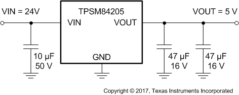 Figure 20. Typical Application
8.2.1 Design Requirements
For this design example, use the parameters listed in Table 3 and follow the design procedures below.
Table 3. Design Parameters
| DESIGN PARAMETER | VALUE |
|---|---|
| Input Voltage VIN | 24-V typical |
| Output Voltage VOUT | 5.0 V |
| Output Current Rating | 1.5 A |
| Key care-abouts | TO-220 footprint, high efficiency |
8.2.2 Detailed Design Procedure
8.2.2.1 Custom Design With WEBENCH® Tools
Click here to create a custom design using the TPSM84203 device with the WEBENCH® Power Designer.
- Start by entering the input voltage (VIN), output voltage (VOUT), and output current (IOUT) requirements.
- Optimize the design for key parameters such as efficiency, footprint, and cost using the optimizer dial.
- Compare the generated design with other possible solutions from Texas Instruments.
The WEBENCH Power Designer provides a customized schematic along with a list of materials with real-time pricing and component availability.
In most cases, these actions are available:
- Run electrical simulations to see important waveforms and circuit performance
- Run thermal simulations to understand board thermal performance
- Export customized schematic and layout into popular CAD formats
- Print PDF reports for the design, and share the design with colleagues
Get more information about WEBENCH tools at www.ti.com/WEBENCH.
8.2.2.2 Input and Output Capacitors
The TPSM842xx devices require both input and output capacitance for proper operation. The minimum required input capacitance for all of the TPSM842xx devices is 10 µF of ceramic capacitance placed directly at the device pins. The minimum required output capacitance for the TPSM84203 and TPSM84205 is 2× 47 µF of ceramic type. The TPSM84212 requires only one 47 µF ceramic output capacitor. Additional capacitance can be added to improve ripple or transient response.
For this application, the minimum required input capacitance of 10 µF, ceramic was added and 2× 47 µF ceramic capacitance was added to the output.
8.2.3 Application Curves
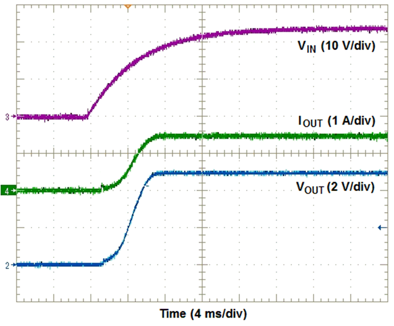
| VIN = 24 V | VOUT = 5 V | IOUT = 1.5 A |
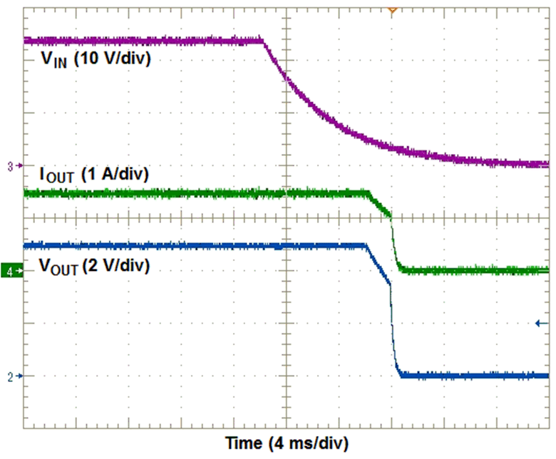
| VIN = 24 V | VOUT = 5 V | IOUT = 1.5 A |
8.2.3.1 EMI
The TPSM842xx devices are all compliant with EN55022 Class B radiated emissions. Figure 23 to Figure 27 show typical examples of radiated emissions plots for the TPSM842xx devices. The EMI plots were taken using a web-orderable EVM with a resistive load. Input power was provided using a lead acid battery. All graphs show plots of the antenna in the horizontal and vertical positions.
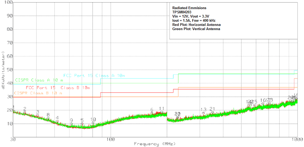
1.5-A Load, Horizontal and Vertical Antenna
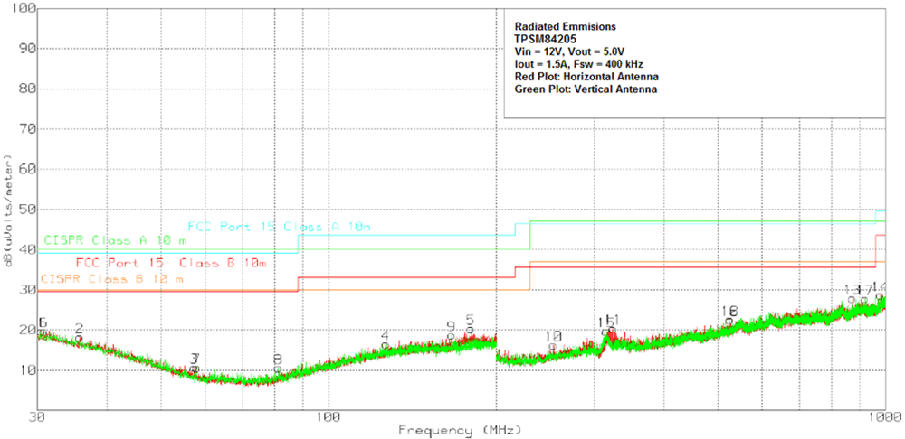
1.5-A Load, Horizontal and Vertical Antenna
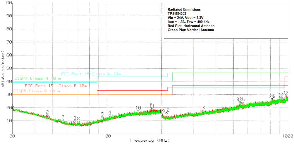 Figure 25. Radiated Emissions 24-V Input, 3.3-V Output,
 1.5-A Load, Horizontal and Vertical Antenna
 Figure 26. Radiated Emissions 12-V Input, 5.0-V Output,
 1.5-A Load, Horizontal and Vertical Antenna
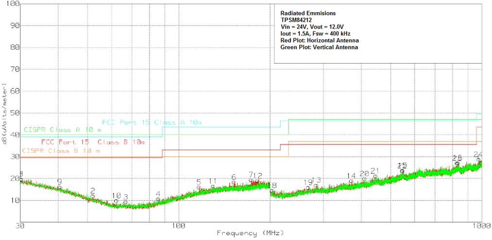 Figure 27. Radiated Emissions 24-V Input, 12-V Output,
 1.5-A Load, Horizontal and Vertical Antenna