SCDS333B June 2012 – July 2016 TS3USB3200
PRODUCTION DATA.
- 1 Features
- 2 Applications
- 3 Description
- 4 Revision History
- 5 Pin Configuration and Functions
- 6 Specifications
- 7 Detailed Description
- 8 Application and Implementation
- 9 Power Supply Recommendations
- 10Layout
- 11Device and Documentation Support
- 12Mechanical, Packaging, and Orderable Information
Package Options
Mechanical Data (Package|Pins)
- RSV|16
Thermal pad, mechanical data (Package|Pins)
Orderable Information
1 Features
- VCC Range: 2.7 V to 4.3 V
- Mobile High-Definition Link (MHL) or Mobility Display Port (MyDP) Switch
- Bandwidth (–3 dB): 5.5 GHz
- Ron (Typical): 5.7 Ω
- Con (Typical): 2.5 pF
- USB Switch
- Bandwidth (–3 dB): 5.5 GHz
- Ron (Typical): 4.6 Ω
- Con (Typical): 2.5 pF
- Current Consumption: 40 µA Typical
- Special Features
- Flexible Power Control: Device Can be Powered by VBUS Without VCC or by VCC Alone
- IOFF Protection Prevents Current Leakage in Powered-Down State (VCC and VBUS= 0 V)
- 1.8-V Compatible Control Inputs (SEL1, SEL2, and PSEL)
- Overvoltage Tolerance (OVT) on All I/O Pins up to 5.5 V Without External Components
- ESD Performance:
- 3.5-kV Human-Body Model (A114B, Class II)
- 1-kV Charged Device Model (C101)
- Package:
- 16-Pin UQFN Package (2.6 × 1.8 mm, 0.4-mm Pitch)
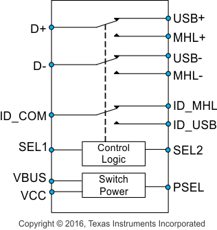
Switch Diagram

2 Applications
- USB 2.0 Applications
- Mobile High-Definition Link (MHL) Applications
- Mobility Display Port (MyDP) Applications
- Mobile Phones
3 Description
The TS3USB3200 is a differential single-pole, double throw (SPDT) multiplexer that includes a high-speed Mobile High-Definition Link (MHL) or Mobility Display Port (MyDP) switch and a USB 2.0 High-Speed
(480 Mbps) switch in the same package. Additionally included is a single-pole, double throw (SPDT) USB/MHL or MyDP ID switch for easy information control. These configurations allow the system designer to use a common USB or Mico-USB connector for both MHL/MyDP video signals and USB data.
The TS3USB3200 has a VCC range of 2.7 V to 4.3 V and also has the option to be powered by VBUS without VCC. The device supports a overvoltage tolerance (OVT) feature which allows the I/O pins to withstand overvoltage conditions (up to 5.5 V). The power-off protection feature forces all I/O pins to be in high impedance mode when power is not present. This allows full isolation of the signals lines without excessive leakage current. The select pins of TS3USB3200 are compatible with 1.8-V control voltage, allowing them to be directly interfaced with the General Purpose I/O (GPIO) from a mobile processor.
The TS3USB3200 comes with a small 16-pin UQFN package (2.6 mm × 1.8 mm in size), which makes it a perfect candidate for mobile applications.
Device Information(1)
| PART NUMBER | PACKAGE | BODY SIZE (NOM) |
|---|---|---|
| TS3USB3200 | UQFN (16) | 2.60 mm × 1.80 mm |
- For all available packages, see the orderable addendum at the end of the data sheet.
4 Revision History
Changes from A Revision (July 2013) to B Revision
- Added ESD Ratings table, Feature Description section, Device Functional Modes, Application and Implementation section, Power Supply Recommendations section, Layout section, Device and Documentation Support section, and Mechanical, Packaging, and Orderable Information section.Go
- Removed Ordering Information table, see POA at the end of the data sheet Go
- Changed Thermal Information table Go
Changes from * Revision (June 2012) to A Revision