SCDS374A September 2017 – September 2017 TS5USBC400
PRODUCTION DATA.
- 1 Features
- 2 Applications
- 3 Description
- 4 Revision History
- 5 Pin Configuration and Functions
- 6 Specifications
- 7 Parameter Measurement Information
- 8 Detailed Description
- 9 Application and Implementation
- 10Power Supply Recommendations
- 11Layout
- 12Device and Documentation Support
- 13Mechanical, Packaging, and Orderable Information
Package Options
Refer to the PDF data sheet for device specific package drawings
Mechanical Data (Package|Pins)
- YFP|12
Thermal pad, mechanical data (Package|Pins)
Orderable Information
8 Detailed Description
8.1 Overview
The TS5USBC400 is a bidirectional low-power dual port, high-speed, USB 2.0 analog switch with integrated protection for USB Type-C systems. The device is configured as a dual 2:1 or 1:2 switch and is optimized for handling the USB 2.0 D+/- lines in a USB Type-C system as shown in Figure 13.
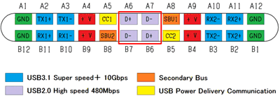 Figure 13. USB Type-C Connector Pinout
The TS5USBC400 also works in traditional USB systems that need protection from fault conditions such as automotive and applications that require higher voltage charging. The device maintains excellent signal integrity through the optimization of both RON and BW while protecting the system with 0 V to 16 V OVP protection. The OVP implementation is designed to protect sensitive system components behind the switch that cannot survive a fault condition where VBUS is shorted the D+ and D- pins on the connector.
8.2 Functional Block Diagram
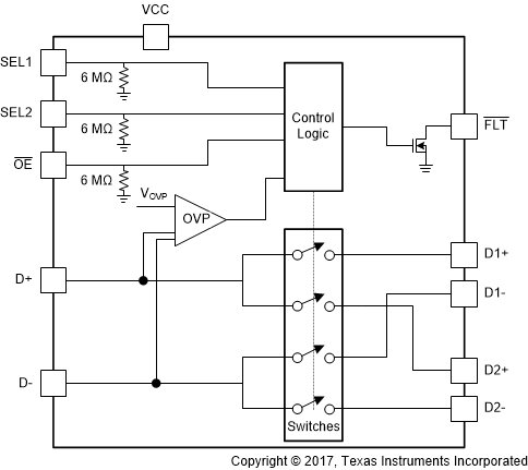
8.3 Feature Description
8.3.1 Powered-off Protection
When the TS5USBC400 is powered off the I/Os of the device remain in a high-Z state. The crosstalk, off-isolation, and leakage remain within the Electrical Specifications.
This prevents errant voltages from reaching the rest of the system and maintains isolation when the system is powering up.
8.3.2 Overvoltage Protection
The OVP of the TS5USBC400 is designed to protect the system from D+/- shorts to VBUS at the USB and USB Type-C connector. Figure 14 depicts a moisture short that would cause 16 V to appear on an existing USB solution that could pass through the device and damage components behind the device.
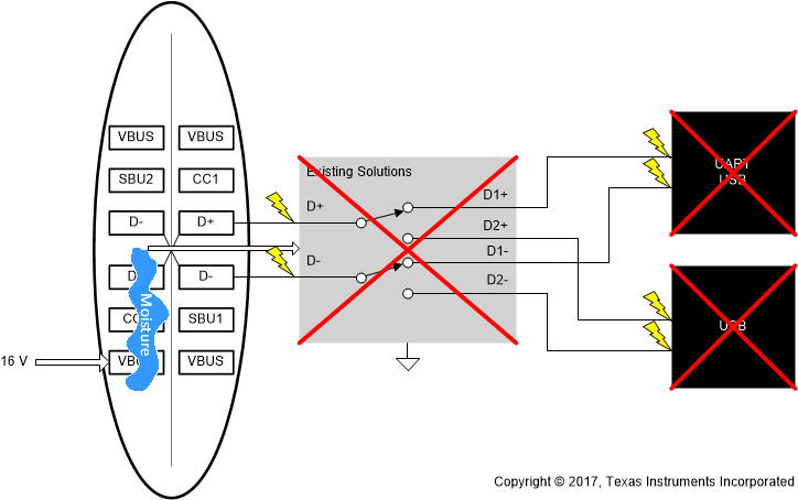 Figure 14. Existing Solution Being Damaged by a Short, 16 V
The TS5USBC400 will open the switches and protect the rest of the system by blocking the 16 V as depicted in .
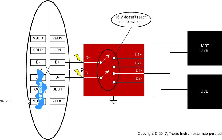 Figure 15. Protecting During a 16-V Short
Figure 16 is a waveform showing the voltage on the pins during an over-voltage scenario.
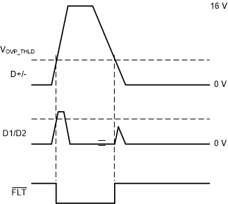 Figure 16. Overvoltage Protection Waveform, 16 V
8.4 Device Functional Modes
8.4.1 Pin Functions
Table 1. Function Table
| OE | SEL1 | SEL2 | D- Connection | D+ Connection |
|---|---|---|---|---|
| H | X | X | High-Z | High-Z |
| L | L | L | D- to D1- | D+ to D1+ |
| L | L | H | D- to D1- | D+ to D2+ |
| L | H | L | D- to D2- | D+ to D1+ |
| L | H | H | D- to D2- | D+ to D2+ |