SCDS375A September 2017 – September 2017 TS5USBC402
PRODUCTION DATA.
- 1 Features
- 2 Applications
- 3 Description
- 4 Revision History
- 5 Pin Configuration and Functions
- 6 Specifications
- 7 Parameter Measurement Information
- 8 Detailed Description
- 9 Application and Implementation
- 10Power Supply Recommendations
- 11Layout
- 12Device and Documentation Support
- 13Mechanical, Packaging, and Orderable Information
Package Options
Refer to the PDF data sheet for device specific package drawings
Mechanical Data (Package|Pins)
- YFP|12
Thermal pad, mechanical data (Package|Pins)
Orderable Information
1 Features
- Supply Range 2.3 V to 5.5 V
- Differential 2:1 or 1:2 Switch/Multiplexer or Flexible Dual Single Ended Cross Switch
- 0-V to 20-V Overvoltage Protection (OVP) on Common Pins
- Powered Off Protection When VCC = 0 V
- Low RON of 9 Ω Maximum
- BW of 1.2 GHz Typical
- CON of 4.5 pF Typical
- Low Power Disable Mode
- 1.8-V Compatible Logic Inputs
- ESD Protection Exceeds JESD 22
- 2000-V Human Body Model (HBM)
- TS5USBC402: Standard Temperature Range of
0°C to 70°C - TS5USBC402I: Industrial Temperature Range of
-40°C to 85°C - Small DSBGA Package
2 Applications
- Mobile
- PC/Notebook
- Tablet
- Anywhere a USB Type-C™ or Micro-B Connector is Used
3 Description
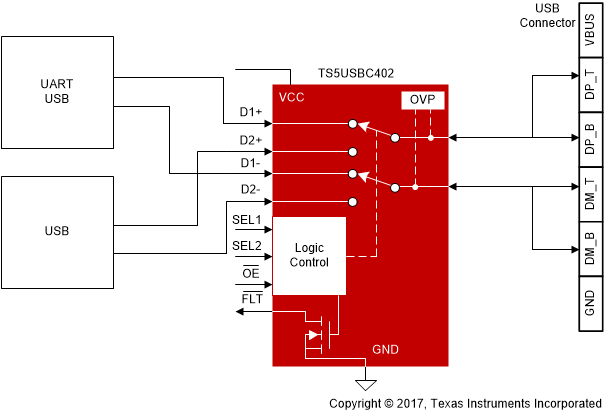
The TS5USBC402 is a bidirectional low-power dual port, high-speed, USB 2.0 analog switch with integrated protection for USB Type-C™ systems. The device is configured as a dual 2:1 or 1:2 switch and is optimized for handling the USB 2.0 D+/- lines in a USB Type-C™ systems.
The TS5USBC402 protection on the I/O pins can tolerate up to 20 V with automatic shutoff circuitry to protect system components behind the switch.
The TS5USBC402 comes in a small 12 pin DSBGA package making it a perfect candidate for mobile and space constrained applications.
Device Information(1)
| PART NUMBER | PACKAGE | BODY SIZE (NOM) |
|---|---|---|
| TS5USBC402 TS5USBC402I |
DSBGA (12) | 1.582 mm × 1.182 mm |
- For all available packages, see the orderable addendum at the end of the data sheet.
Simplified Schematic
